These variations in
clock signals between various network elements may cause a loss of data downstream from the sender if the
clock signal at which data is written to the synchronous
payload and the
clock signal at which the data is read from the synchronous payload are sufficiently different.
For example,
network clock instability, electrical
noise and interference, effective changes in the length of transmission media, changes in the velocity of propagation, Doppler shifts, irregular timing information, and other electrical and network problems may all cause clock variations.
An aperiodic or non-periodic pointer adjustment may be bursty in nature when caused by a transient problem or condition within the network.
Jitter refers to the phase variations in the
clock signal, which may cause errors in identifying bit positions and values accurately, and is therefore an issue in synchronous systems.
A PLL is most effective at filtering out
high frequency jitter components, i.e., those with a frequency greater than 10 Hz, but is less effective at filtering out the
low frequency wander components.
In addition, the large time constants required would result in a PLL that is slow to lock onto the reference
signal and would cause long delays in recovering lock after a transient event.
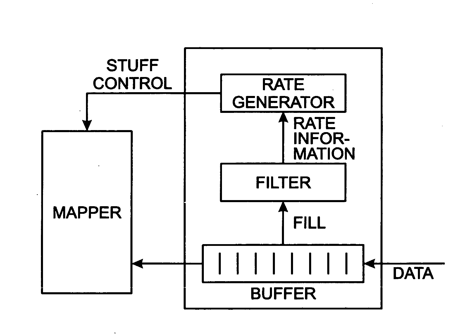
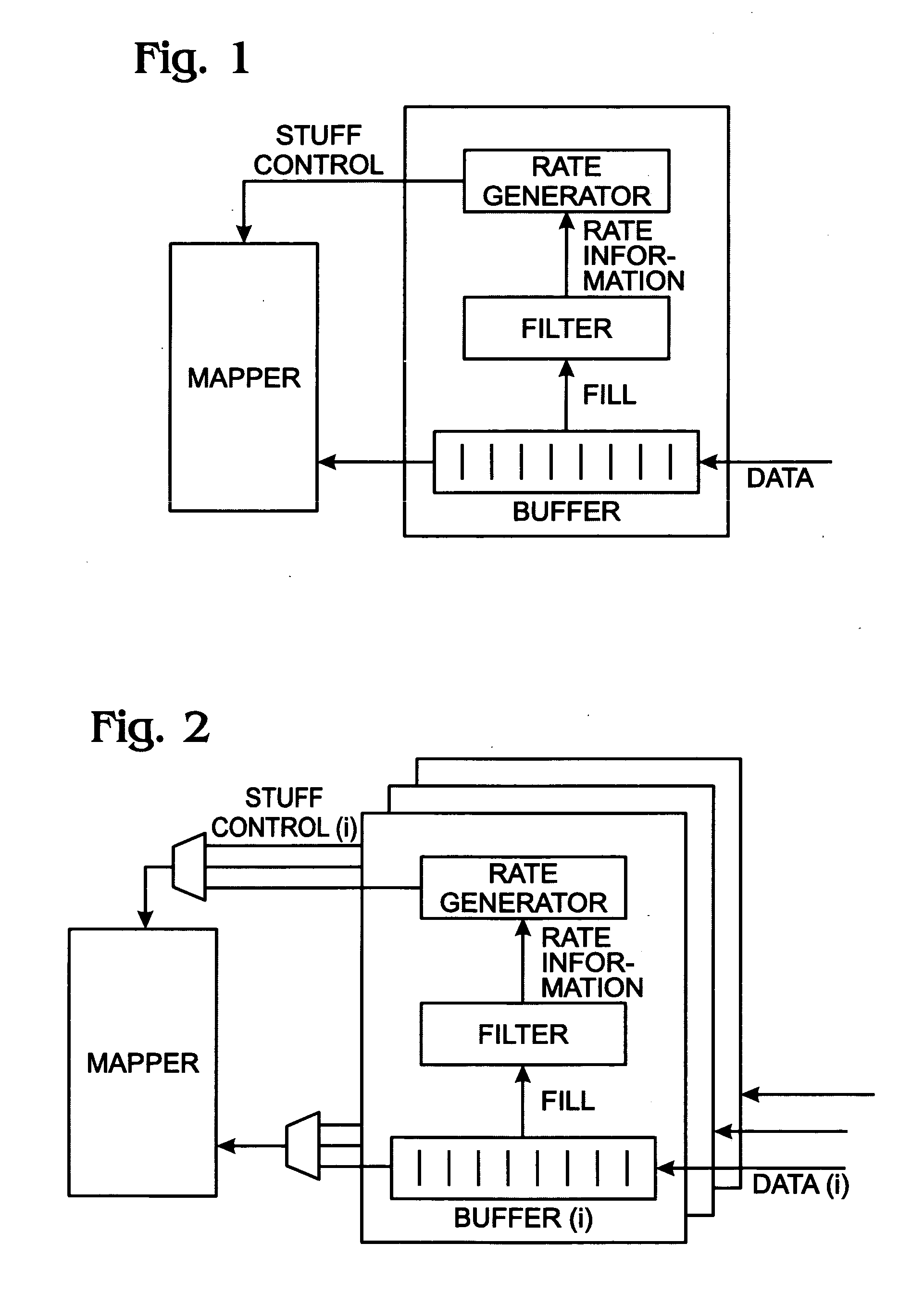
One source of wander errors in the output
data rate can be caused by the pointer adjustments within the synchronous signals.
Each pointer adjustment signal or asynchronous gap data results in a data gap for a given number of clock cycles.
The inconsistent nature of the gapped data can result in large changes in the data output rate.
Data overflow occurs when data is written to the elastic store at a faster rate than usual, or read at a slower rate than usual, causing the elastic store to accumulate data.
In these conditions, the elastic store may be unable to store all of the incoming data, and data may be lost.
Similarly, data underflow occurs when data is written to the elastic store at a slower rate than usual, or read at a faster rate than usual, causing the elastic store to lose data.
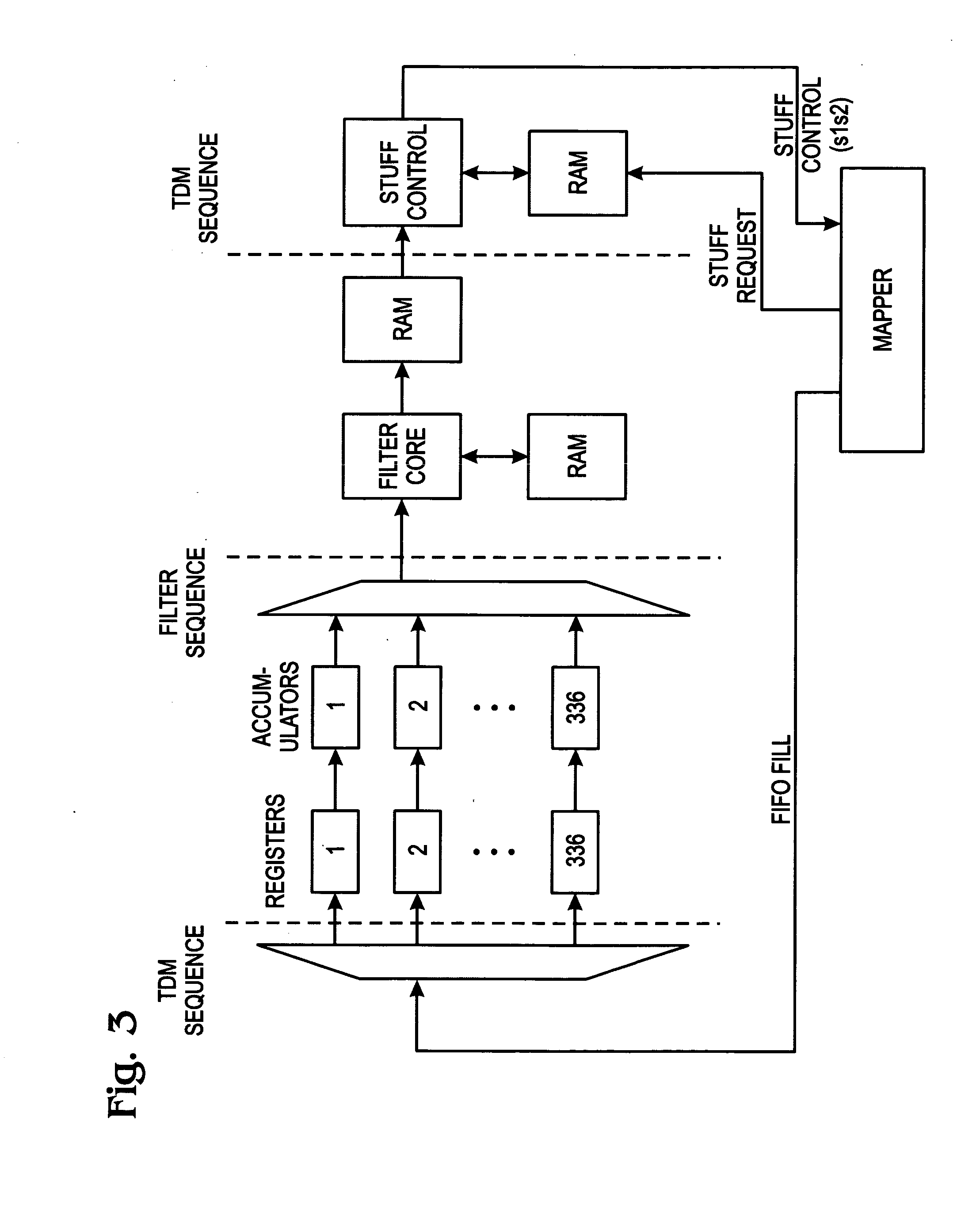
Similar problems related to the
processing of the VT pointer bytes occur, and the positive justification of the VT pointer bytes is accomplished by assigning the bytes immediately after the V3 bytes as positive stuff opportunity bytes.
In addition, the wander and
jitter associated with the pointer adjustments is also uncorrelated between the transport overhead pointer bytes and the VT overhead pointer bytes.
The highly non-uniform input
data rate to a SONET SPE is primarily due to the presence of transport overhead (TOH) and the position of
data bits and stuff bits in the SONET SPE.
Thus, there may be long gaps with no data when TOH data is present.

