
Semiconductor memory device

a memory device and semiconductor technology, applied in static storage, digital storage, instruments, etc., can solve the problems of increasing system cost and package area, difficult to set the word line voltage at a read time to be sufficiently high, and the nand-type flash memory is not suitable for high-speed random access use, etc., to achieve the effect of small capacitan

Inactive Publication Date: 2008-04-03
KK TOSHIBA
View PDF12 Cites 131 Cited by
  • Summary
  • Abstract
  • Description
  • Claims
  • Application Information

AI Technical Summary

Benefits of technology

[0024]the first data area serves as such a sequential access-use bank that a sector defined by a certain number of bits serves as an access unit while the second data

Problems solved by technology

NAND-type flash memories are not suitable for a high speed random access use because the cell current is small, i.e., about one dozens in comparison with that of NOR-type flash memories.
Further, in the multi-level data storage scheme, it is difficult to set a word line voltage at a read time to be sufficiently higher in comparison with the cell threshold voltage, and the cell current is not more than about several hundreds nA.
However, in case the above-described two-chip configuration with a NOR-type flash memory and a NAND-type flash memory is used, both of the system cost and the package area increase.
Therefore, the NAND-type flash memory is not adaptable to random access necessary for a CPU when executing a program such as OS.

Method used


Image

  • Semiconductor memory device
  • Semiconductor memory device
  • Semiconductor memory device

Examples


Embodiment Construction

[0046]Illustrative embodiments of this invention will be explained with reference to the accompanying drawings below.

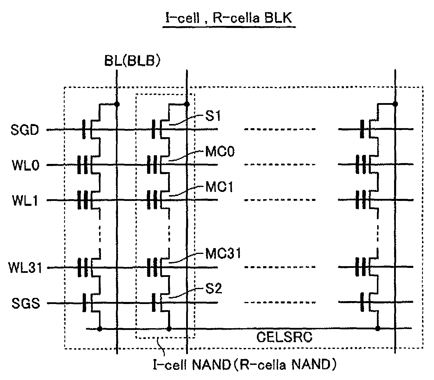
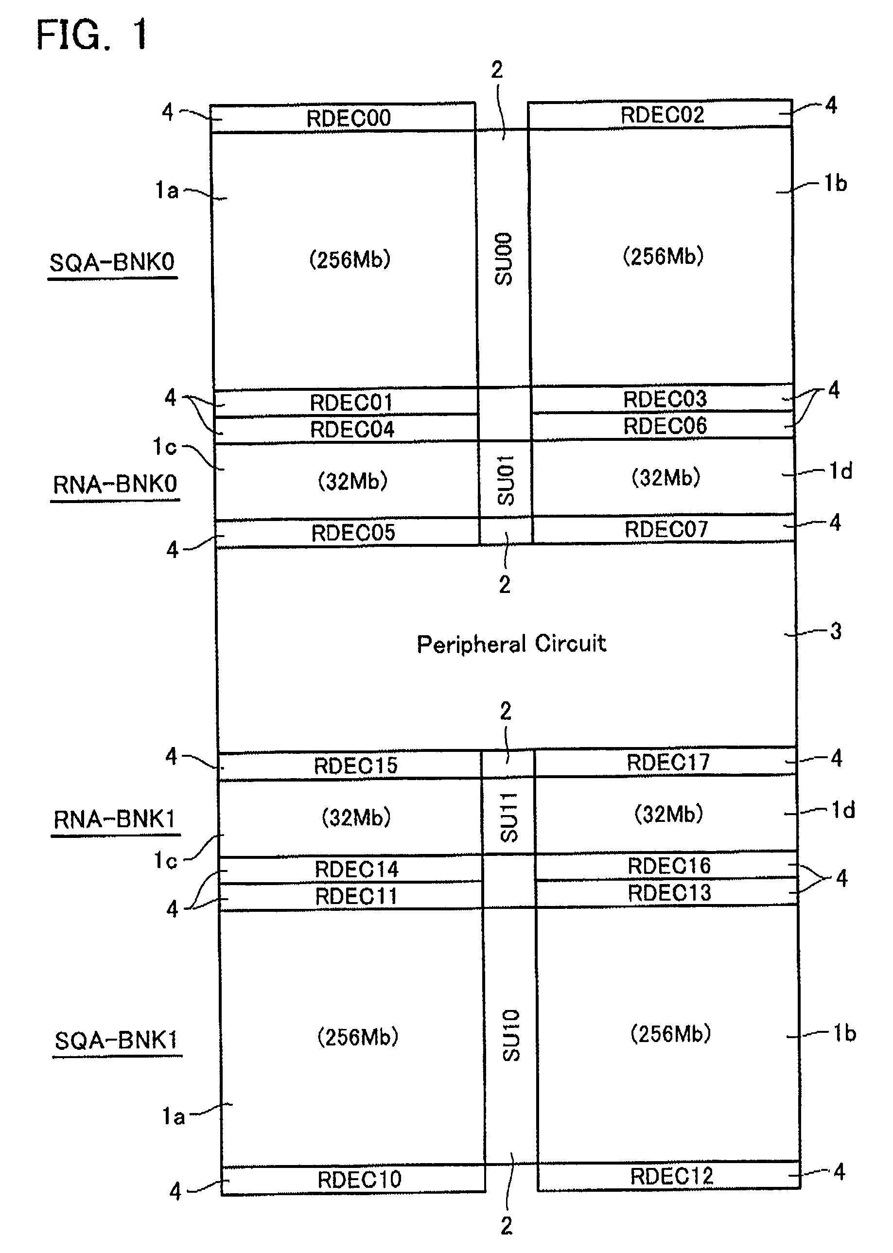
[0047]FIG. 1 shows an outlined layout of a NAND-type flash memory chip in accordance with this embodiment. This memory hip contains banks, RNA-BNKi and SQA-BNKi. RNA-BNKi is a random accessible data area while SQA-BNKi is a sequential accessing data area with a capacity larger than RNA-BNKi.

[0048]A center portion of the chip is a peripheral circuit area 3. High-speed random-access-use banks RNA-BNK0 and RNA-BNK1 are disposed to sandwich the peripheral circuit portion 3. Further disposed outside the random access-use banks RNA-BNK0 and RNA-BNK1 are sequential access-use banks SQA-BNK0 and SQA-BNK1, which are sequentially accessed in such a way that a sector defined by a certain number of bits serves as an access unit.

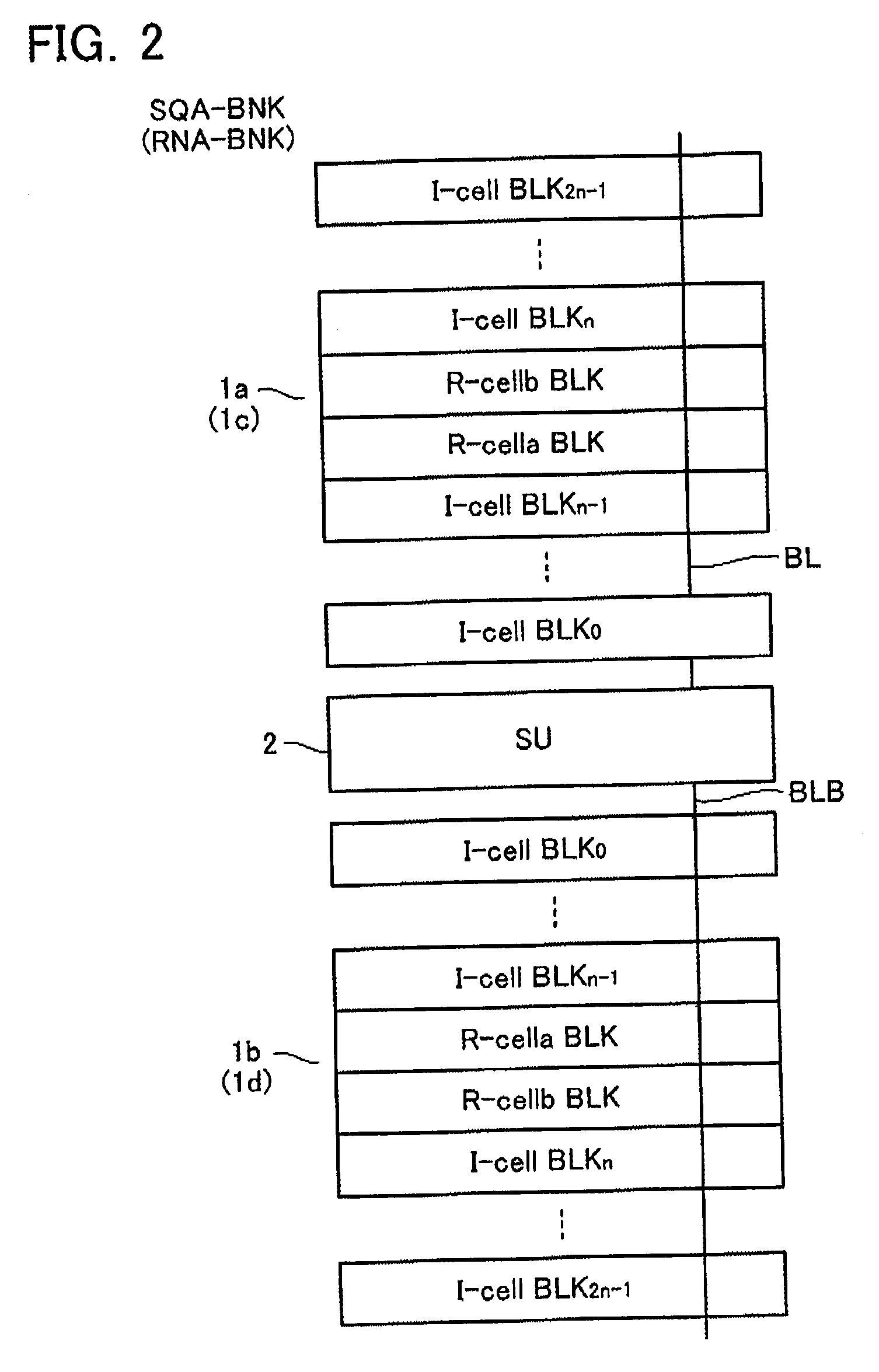
[0049]Each of random access-use banks RNA-BNK0 and RNA-BNK1 is formed of two cell arrays 1c and 1d, which are disposed to sandwich sense units (SU01, SU11...


PUM


Abstract

There is provided a semiconductor memory device with NAND strings arranged therein, the NAND string having a plurality of electrically rewritable and non-volatile memory cells connected in series, including: a first data area; and a second data area, which is smaller in capacitance than the first data area and random accessible at a higher rate than the first data area.

Description

CROSS-REFERENCE TO RELATED APPLICATION[0001]This application is based on and claims the benefit of priority from the prior Japanese Patent Application No. 2006-266145, filed on Sep. 29, 2006, the entire contents of which are incorporated herein by reference.BACKGROUND OF THE INVENTION[0002]1. Field of the Invention[0003]This invention relates to a semiconductor memory device, in which two data areas, i.e., a high-speed accessing area and a large capacity storing area, are set.[0004]2. Description of the Related Art[0005]There is increased a demand for NAND-type flash memories in accordance with increasing of the demand for mobile devices, which deal with large capacitive data such as a still or moving image. In the recent flash memories, since it is used such a multi level data storage scheme that two or more bits are stored in one memory cell, it has become possible to store a quantity of information with a relatively small chip area.[0006]NAND-type flash memories are not suitable ...

Claims


Application Information

Patent Timeline
IPC IPC(8): G11C16/04
CPCG11C2211/5641G11C11/5642
Inventor EDAHIRO, TOSHIAKISUZUKI, TOSHIHIROTODA, HARUKI
Owner KK TOSHIBA
Features
  • Generate Ideas
  • Intellectual Property
  • Life Sciences
  • Materials
  • Tech Scout
  • Unparalleled Data Quality
  • Higher Quality Content
  • 60% Fewer Hallucinations
Learn More