Processes and packaging for high voltage integrated circuits, electronic devices, and circuits

a technology of integrated circuits and processing equipment, applied in the direction of semiconductor devices, electrical apparatus, semiconductor/solid-state device details, etc., can solve the problems of only achieving greater densities at the pcb level, requiring careful attention to physical layout, and requiring circuits to be operated with care, so as to reduce thickness and reduce thickness

Inactive Publication Date: 2008-04-03
INNOVATE LLC
View PDF13 Cites 24 Cited by
  • Summary
  • Abstract
  • Description
  • Claims
  • Application Information

AI Technical Summary

Benefits of technology

[0014]An embodiment of a method of packaging integrated circuits is also disclosed. The method may include providing a processed semiconductor wafer with electronics fabricated thereon. The method may further include optionally grinding the processed semiconductor wafer to reduce thickness. The method may include dicing the processed semiconductor wafer to physically separate the electronics into dice. The method may include bonding the dice to an electronics package. The method may include electrically connecting the dice to each other and to the electronics package. The method may include back-filling gaps between and around the dice and sealing the electronics package to provide a packaged integrated circuit.
[0015]An embodiment of a method of flip-chip packaging integrated circuits according to the present invention is disclosed. The method may include providing a processed semiconductor wafer having electronics fabricated on an electronics side and bulk semiconductor on a substrate side. The method may further include optionally grinding the substrate side to reduce thickness. The method may further include bonding a stacked wafer to the substrate side and applying under-bump metallization to the electronics side. The method may further include dicing the processed semiconductor wafer to physically separate the electronics into dice and separating at least one of the dice as an electronics module. The method may further include flip-chip bonding the electronics module to a flip-chip carrier. The method may further include coating the electronics module with an insulator and optionally under-filling gaps between the electronics module and the flip-chip carrier.

Problems solved by technology

However, high voltage electronics require careful attention to physical layouts when formed on semiconductor substrates and when mounting on PCBs.
This is because the high voltages may cause arcing to nearby components, or circuit traces and thereby cause malfunction and / or damage to the circuits.
However, the EIHatem et al. approach only achieves greater densities at the PCB level.
However, such series stacking configurations generally require high voltage resistors for correctly biasing gate voltages through a voltage divider network and other means.
Even in integrated form, high voltage resistors are bulky.
However, Hu et al. does not appear to disclose the formation of individual circuits on a substrate, separating the individual circuits on the substrate, dicing a module from the separated individual circuits, isolating the module, making connections on the module and back-filling to further isolate the individual circuits and to achieve high breakdown voltage, Vbd.
If even one of the coating materials is missing or defective the voltage sustainable by the packaging drops dramatically and reliability of the parts will be severely downgraded.” Col. 4, II.

Method used


Image

  • Processes and packaging for high voltage integrated circuits, electronic devices, and circuits
  • Processes and packaging for high voltage integrated circuits, electronic devices, and circuits
  • Processes and packaging for high voltage integrated circuits, electronic devices, and circuits

Examples


Embodiment Construction

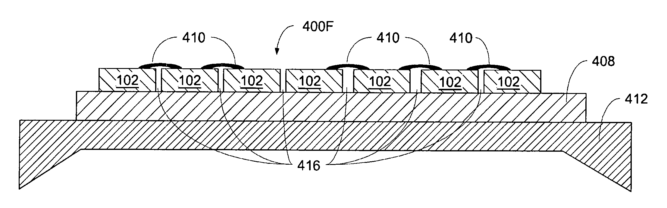
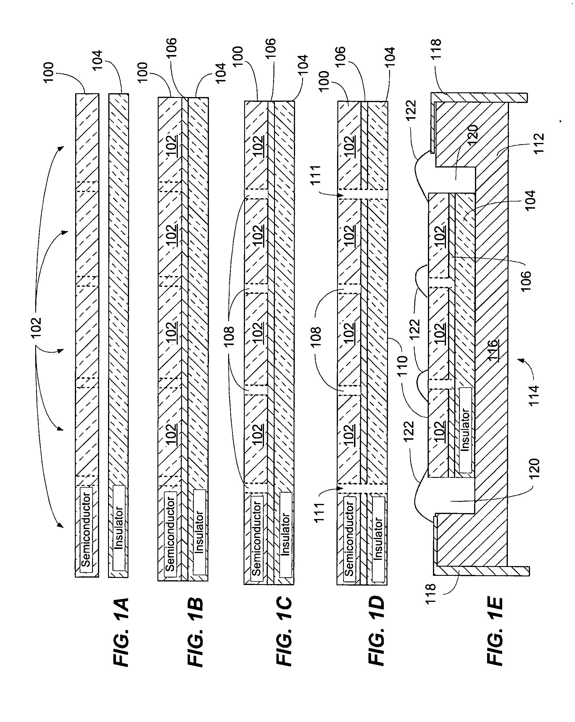
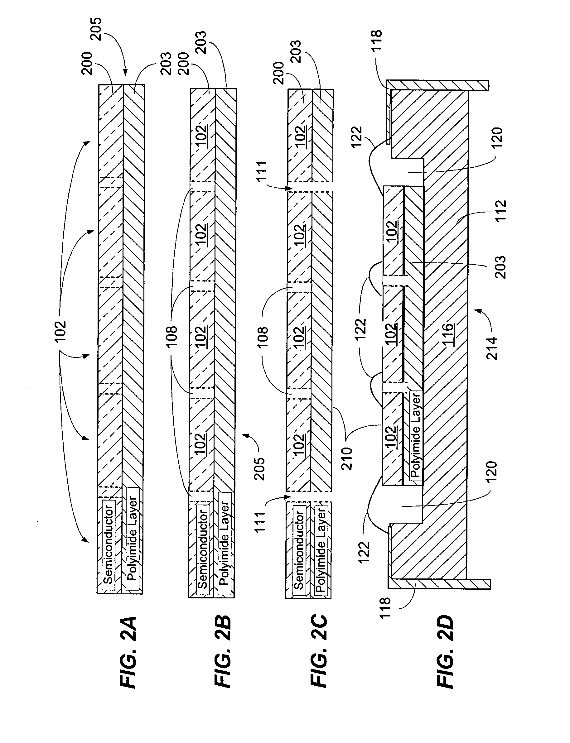
[0027]Reference will now be made to figures of embodiments of the present invention, wherein like structures will be provided with like reference designations. It is understood that the drawings are diagrammatic and schematic representations of exemplary embodiments of the present invention and are neither limiting of the present invention nor are they necessarily drawn or shown to scale.

[0028]FIGS. 1A-1E are illustrations of an embodiment of a process for packaging integrated circuits using insulators according to the present invention. The process disclosed below allows high breakdown voltages, e.g., thousands of volts, to be achieved from individual transistors. Integrated circuits formed according to the process illustrated in FIGS. 1A-1E are particularly suitable for high voltage electronics with high breakdown voltage, Vbd.

[0029]Referring to FIG. 1A, a semiconductor 100 may be provided with electronics, shown generally at 102. The semiconductor 100 may be formed of silicon, ge...


PUM


Abstract

The present invention includes processes and packaging for high voltage integrated circuits (ICs), high voltage electronic devices and high voltage electronic circuits which operate over a wide range of voltages, e.g., from tens of volts to tens of thousands of volts. The inventive processes and packaging are particularly suitable for integrating low or lower voltage circuits or transistors to form high voltage ICs, high voltage electronic devices and high voltage electronic circuits. The inventive processes and packaging are also particularly suitable for isolating high voltage electronics to achieve high breakdown voltages and for supporting high voltage operation. The inventive processes may be used with any suitable semiconductor materials using conventional semiconductor fabrication and related facilities.

Description

BACKGROUND OF THE INVENTION[0001]1. Field of the Invention[0002]The present invention relates generally to processes and packaging for high voltage integrated circuits (ICs), electronic devices and high voltage electronic circuits. More particularly, this invention relates to processes for fabrication and manufacturing of high voltage integrated electronics that are capable of voltage operation in a range of tens of volts to tens of thousands of volts.[0003]2. Description of Related Art[0004]High voltage integrated circuits (ICs), electronic devices and circuits find many applications. High voltage ICs, high voltage electronic devices and circuits may be used to replace bulky discrete electronic components such as individual high voltage transistors, resistors and transformers. Additionally, it is desirable to integrate these generally bulky discrete high voltage components directly on silicon, in a package, or on a printed circuit board (PCB) to achieve greater miniaturization, hig...

Claims


Application Information

Patent Timeline
Patent Type & Authority Applications(United States)
IPC IPC(8): H01L21/336
CPCH01L21/561H01L21/6835H01L21/78H01L24/18H01L24/27H01L24/28H01L24/32H01L24/48H01L24/80H01L24/82H01L24/83H01L24/94H01L24/96H01L24/97H01L25/0655H01L25/50H01L2221/68322H01L2224/18H01L2224/2919H01L2224/48091H01L2224/48137H01L2224/48227H01L2224/48247H01L2224/484H01L2224/73265H01L2224/76155H01L2224/83101H01L2224/8385H01L2224/8592H01L2224/97H01L2924/01005H01L2924/01007H01L2924/01013H01L2924/01014H01L2924/01025H01L2924/01027H01L2924/01028H01L2924/01031H01L2924/01032H01L2924/01078H01L2924/01079H01L2924/01082H01L2924/01322H01L2924/07802H01L2924/09701H01L2924/14H01L2924/15153H01L2924/15165H01L2924/1517H01L2924/16195H01L2924/19043H01L2924/01006H01L2924/01023H01L2924/01033H01L2924/0665H01L2224/32245H01L2924/10253H01L2224/82102H01L2924/1461H01L2924/00014H01L2224/82H01L2924/00H01L2924/15787H01L2924/181H01L2924/18162H01L24/24H01L2224/24137H01L2224/95136H01L2224/2612H01L2224/45099H01L2224/05599
Inventor SADWICK, LAURENCE P.MOJARRADI, MOHAMMAD M.HWU, RUEY-JENCHERN, JEHN-HUAR
Owner INNOVATE LLC
Why Eureka
Try Eureka