Flexible printed circuit board

a printed circuit board and flexible technology, applied in the direction of dielectric characteristics, high frequency circuit adaptations, electrical apparatus construction details, etc., can solve the problems of increased transmission loss, difficult transmission of signals at high frequency bands, increased transmission loss, etc., to increase conductive resistance and increase transmission loss

Inactive Publication Date: 2008-04-10
YAMAICHI ELECTRONICS
View PDF3 Cites 16 Cited by
  • Summary
  • Abstract
  • Description
  • Claims
  • Application Information

AI Technical Summary

Benefits of technology

[0010]As shown in FIG. 11A, when the ground layer 4 is formed, the impedance matching is necessary for assuring the flexibility of the flexible printed circuit board under the condition wherein the thickness of the insulative substrate 6 is relatively thin. For the impedance matching, however, it is required to make a width of the respective dielectric layer 8b (a wire diameter of the signal line) to be smaller, resulting in the increase in conductive resistance. This increases the transmission loss, and there may be a risk in that the transmission of signals at a high frequency band is difficult when a length of the flexible printed circuit board is relatively longer.
[0011]As shown in FIG. 11B, if the respective dielectric layers 20b are enclosed via the dielectric layers 16 and 24, the effective relative permittivity and the dielectric loss coming from a dielectric increase. Further, as described above, since the metallic covering layers 14 and 26 must be connected to each other via a plurality of through-holes not shown to equalize the potentials thereof to each other, the number of processes for producing the flexible printed circuit board increase to raise the production cost.
[0013]By taking such problems into consideration, an object of the present invention is to provide, at a low production cost, a flexible printed circuit board for electrically connecting electric equipments to each other, without increasing a loss of signal transmission even if a length of the flexible printed circuit board is relatively long.
[0016]As apparent from the above-mentioned explanation, according to the flexible printed circuit board of the present invention, since the reticulate covering member formed of porous dielectric covers the insulative substrate to reduce the electrical interference, there is no risk of increase in transmission loss even if a length of the flexible printed circuit board is relatively long. In addition, the production cost thereof is not expensive.

Problems solved by technology

This increases the transmission loss, and there may be a risk in that the transmission of signals at a high frequency band is difficult when a length of the flexible printed circuit board is relatively longer.
Accordingly, as mentioned above, there is a risk in that the transmission loss increases and the transmission of signals at a high frequency band becomes difficult.

Method used


Image

  • Flexible printed circuit board
  • Flexible printed circuit board
  • Flexible printed circuit board

Examples


first embodiment

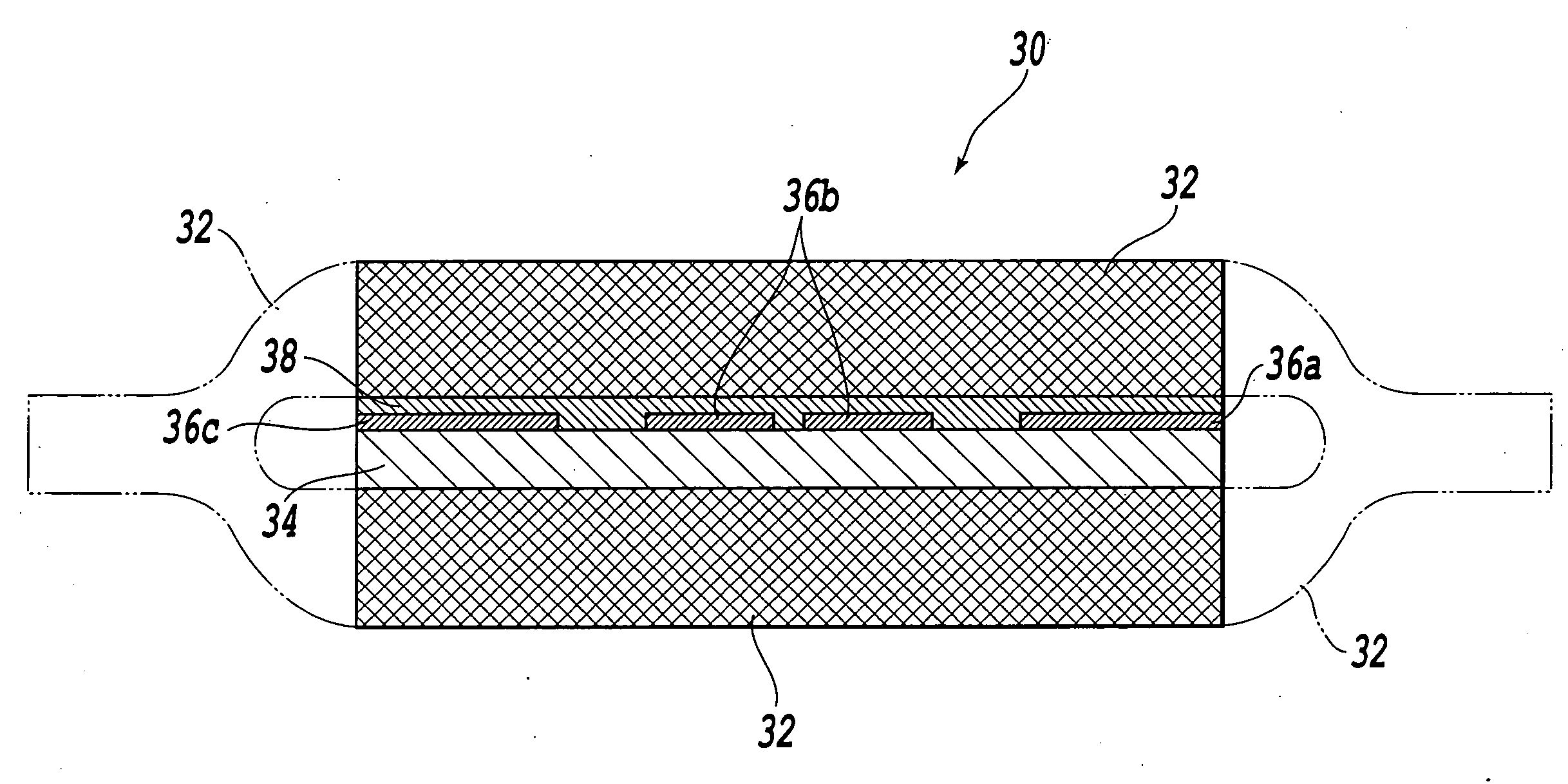
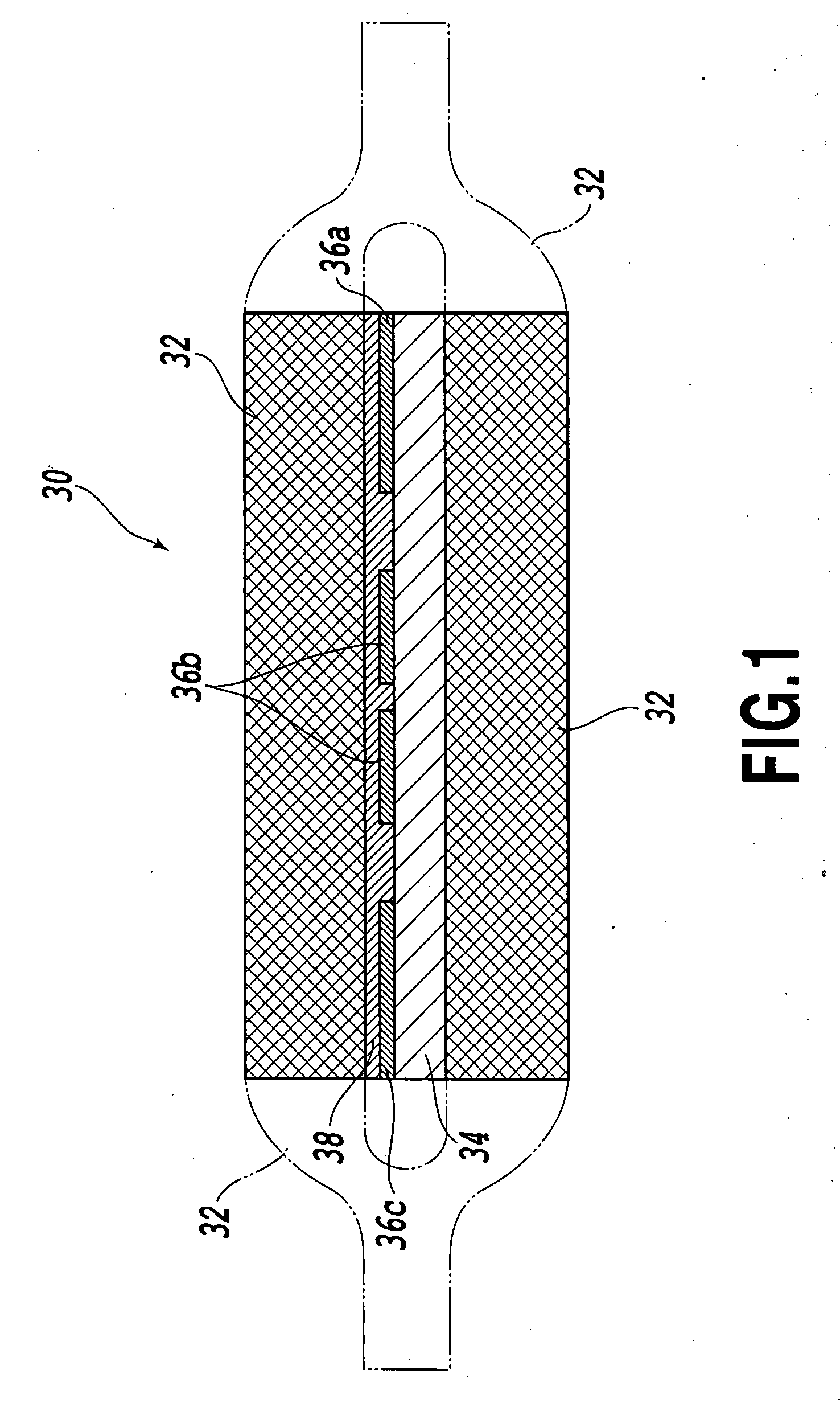
[0029]FIGS. 1 and 2 illustrate a main part of a flexible printed circuit board according to the present invention.

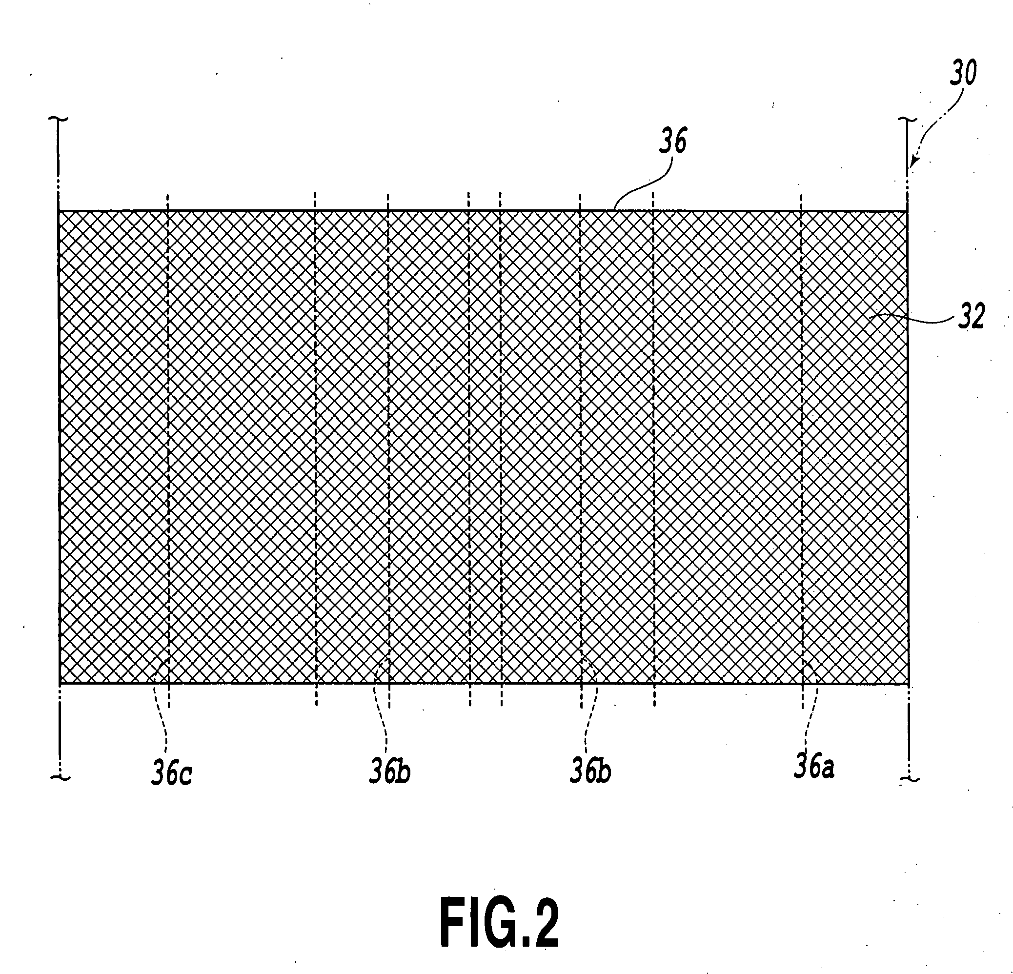
[0030]In FIG. 1, the flexible printed circuit board 30 includes an insulative substrate 34 having a plurality of conductive layers 36a, 36b and 36c covered with a protective layer 38 on one surface, and a mesh-cloth member 32 which is a reticulate covering member encircling all of the protective layer 38 and the insulative substrate 34. Note in FIGS. 1 and 2, a part of the flexible printed circuit board 30 having a predetermined length is illustrated in enlarged dimension.

[0031]The insulative substrate 34 is molded, for example, with glass-epoxy resin, liquid crystal polymer or others to be approximately 50 μm thick. On the other hand, the plurality of conductive layers 36a, 36b and 36c are formed of copper alloy by a known pattern-forming technique. Two conductive layers 36b extend generally parallel to each other vertical to a paper surface and form signal lines. The c...

second embodiment

[0058]FIG. 3A illustrates a main part of a flexible printed circuit board according to the present invention.

[0059]A flexible printed circuit board 40 shown in FIG. 3A has metallic covering layers 42A and 42B of a predetermined thickness on the outer circumference of the mesh-cloth members 32 of the flexible printed circuit board 30 shown in FIG. 1, in addition thereto.

[0060]In FIG. 3A, the same reference numerals are used for designating the same constituent elements as in FIG. 1, and the explanation thereof will be eliminated.

[0061]The metallic covering layers 42A and 42B are formed of a copper tape having adhesive on one surface of copper foil of 10 μm thick or an aluminum tape having adhesive on one surface of aluminum foil of 10 μm thick, while taking a skin effect into consideration.

[0062]Ends of the covering layers 42A and 42B in the extending direction of the ground conductive layers 36a and 36c are respectively connected to ends of the latter not shown. In this regard, it i...


PUM

PropertyMeasurementUnit
relative dielectric constantaaaaaaaaaa
porosityaaaaaaaaaa
thicknessaaaaaaaaaa

Abstract

A flexible printed circuit board wherein the insulative substrate 34 having a plurality of conductive layers 36b covered with a protective layer 38 is encircled by a mesh-cloth member 32.

Description

[0001]This application claims the benefit of Japanese Patent Application No. 2006-275324, filed Oct. 6, 2006, which is hereby incorporated by reference herein in its entirety.FIELD OF THE INVENTION[0002]The present invention relates to a flexible printed circuit board for the mutual electrical connection of electrical components.DESCRIPTION OF THE RELATED ART[0003]Regarding the mutual electrical connection of electrical components, a flexible printed circuit board (FPC) is in practical use as disclosed in Japanese Patent Laid-Open NO. 2000-269612. This flexible printed circuit board 2 has a structure wherein a plurality of conductive layers 8a, 8b and 8c covered with a protective layer 10 are formed on one surface of an insulative substrate 6 e.g. as shown in FIG. 11A.[0004]The insulative substrate 6 is molded with glass-epoxy resin, for example. Also, the conductive layers 8a, 8b and 8c are formed from e.g. a layer of a copper alloy. The protective layer 10 is formed out of a heat-...

Claims


Application Information

Patent Timeline
Patent Type & Authority Applications(United States)
IPC IPC(8): H05K1/00
CPCH05K1/0218H05K1/024H05K1/0393H05K2201/0715H05K2201/0116H05K2201/029H05K3/281H05K1/02
Inventor KUSAMITSU, HIDEKI
Owner YAMAICHI ELECTRONICS
Why Eureka
Try Eureka