Adjustable electrodes and coils for plasma density distribution control

Inactive Publication Date: 2008-04-10
TAIWAN SEMICON MFG CO LTD
View PDF10 Cites 183 Cited by
  • Summary
  • Abstract
  • Description
  • Claims
  • Application Information

AI Technical Summary

Problems solved by technology

It is becoming more difficult to satisfy advanced semiconductor process requirements in terms of uniformity of etch rate, etch profile, CDU, etch selectivity, residue, deposition rate and so on, using current semiconductor process tools, equipment and methods.
Current tools, equipment and methods are generally incapable of achieving the requirements for 45 nanometer (nm) and smaller process techno

Method used


Image

  • Adjustable electrodes and coils for plasma density distribution control
  • Adjustable electrodes and coils for plasma density distribution control
  • Adjustable electrodes and coils for plasma density distribution control

Examples


Embodiment Construction

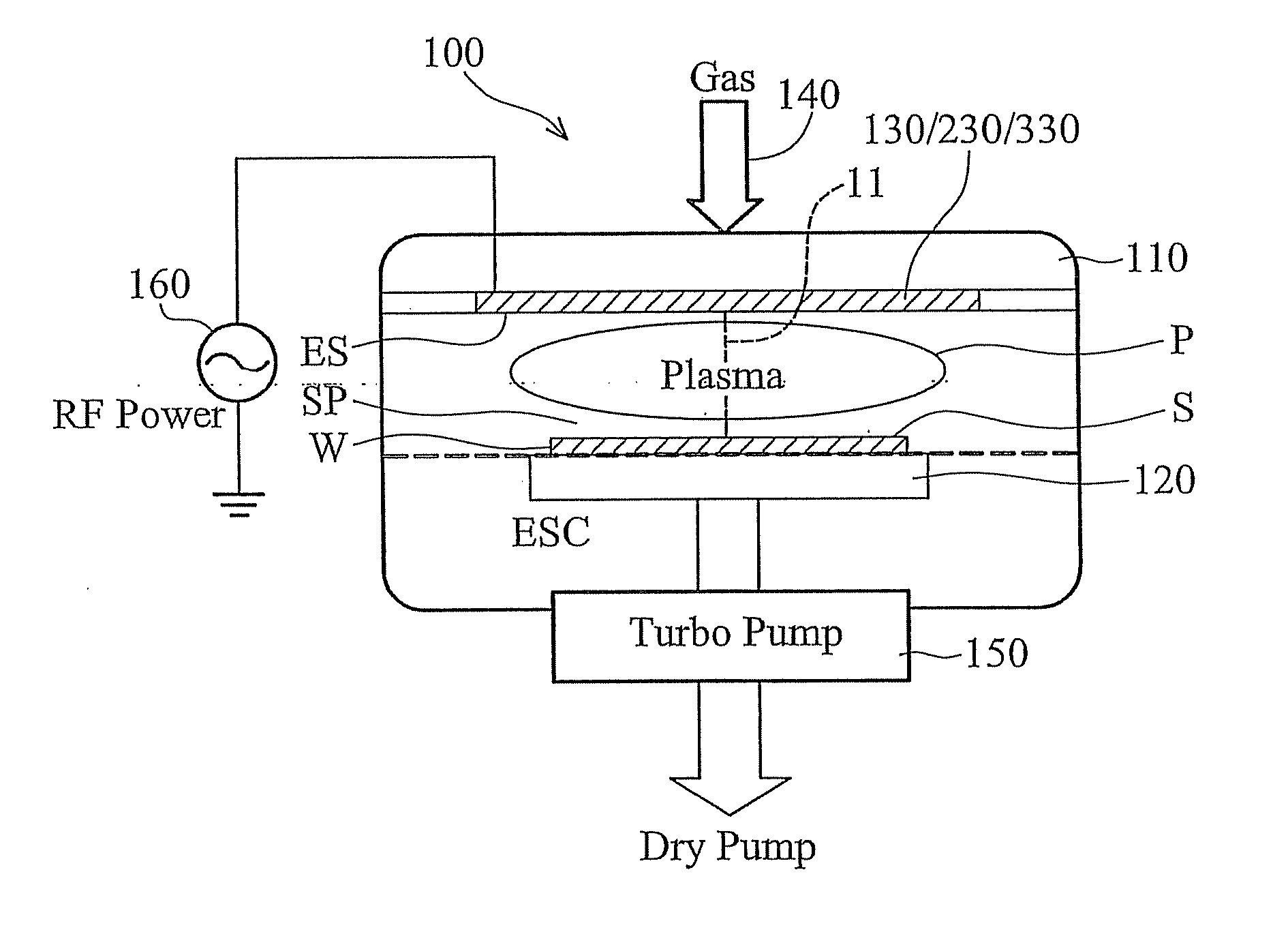
[0030]Disclosed herein is an adjustable upper electrode or coil for an apparatus of the type which may be used in the dry processing of semiconductor wafers and other wafers and substrates. The adjustable electrode or coil may be used in any dry processing or like apparatus that uses an upper electrode or coil including, for example but not limited to, parallel-plate plasma reactors.

[0031]FIG. 1 is a cross-sectional schematic of an embodiment of a parallel-plate plasma reactor 100 for a dry process reactor system, having an adjustable upper electrode for ion plasma density distribution control capability. The plasma reactor 100 may be used in semiconductor fabrication for performing various semiconductor processes, such as dry etching, chemical vapor deposition (CVD), or diffusion. The plasma reactor 100 may comprise a pressure reaction chamber 110 capable of being heated to a temperature ranging, for example, between about 20° C. to about 300° C., and a wafer holder 120 having in a...


PUM

PropertyMeasurementUnit
Diameteraaaaaaaaaa
Densityaaaaaaaaaa
Shapeaaaaaaaaaa

Abstract

A adjustable upper coil or electrode for a reaction chamber apparatus useable in semiconductor processing, is constructed so that its shape may be selectively changed or so at least two portions thereof may be selectively driven at different power and/or frequencies. The adjustable upper coil or electrode, therefore, enables the plasma density distribution in the reaction chamber apparatus to be selectively controlled.

Description

FIELD OF THE INVENTION[0001]The invention relates to semiconductor fabrication. In particular, the present invention relates to adjustable electrodes and coils for controlling the plasma density distribution in a dry processing apparatus.BACKGROUND OF THE INVENTION[0002]Uniformity control across a semiconductor wafer is becoming more important, especially through nanometer technology. It is becoming more difficult to satisfy advanced semiconductor process requirements in terms of uniformity of etch rate, etch profile, CDU, etch selectivity, residue, deposition rate and so on, using current semiconductor process tools, equipment and methods. Current tools, equipment and methods are generally incapable of achieving the requirements for 45 nanometer (nm) and smaller process technology, and / or 300 mm (˜12-inches in diameter) and larger wafers.[0003]For example, dry process reactor systems are used in semiconductor fabrication for performing various semiconductor processes, such as etchi...

Claims


Application Information

Patent Timeline
IPC IPC(8): B23K9/00
CPCH01J37/32091H01J37/32568H01J37/321
Inventor CHEN, YING-LINKAO, CHI-ANCHEN, PO-ZENHSIAO, YI-LIYU, CHEN-HUAWANG, JEANSHEU, LAWRANCE
Owner TAIWAN SEMICON MFG CO LTD
Why Eureka
Try Eureka