Lead frame for an optical semiconductor device, optical semiconductor device using the same, and manufacturing method for these

a technology for optical semiconductor devices and lead frames, applied in semiconductor devices, solid-state devices, basic electric elements, etc., can solve the problems of insufficient optical semiconductor devices, achieve the effect of reducing and/or suppressing the formation of agcl, reducing the risk of discoloration, and improving conventional technology

Inactive Publication Date: 2008-04-10
PANASONIC CORP
View PDF16 Cites 28 Cited by
  • Summary
  • Abstract
  • Description
  • Claims
  • Application Information

AI Technical Summary

Benefits of technology

[0015]The present invention has been achieved in light of the above problem, and aims to provide a lead frame for an optical semiconductor device, an optical semiconductor device using such lead frame, and a manufacturing method for these, where the optical semiconductor device exhibits favorable brightness over a long period of time by preventing discoloration and degeneration of a plating layer provide on the lead frame and a resulting reduction in a reflection coefficient for light emitted from a light emitting element, even when using silicone resin as a sealing resin.
[0032]According to the structures of the lead frame and optical semiconductor device of the present invention, the pure Ag plating layer, which is formed on the surface of the lead frame as a part of the plating layer stack, is covered at all times by a resistant plating layer such as the Ag—Au alloy plating layer. Therefore, in the optical semiconductor device of the present invention, when sealing resin such as silicone resin is adhered to an area of the lead frame where the plating layer stack has been formed, contact between the lone Ag component of the pure Ag plating layer and the silicone resin or other sealing resin is avoided. Such an innovation enables preventing the Ag component of the pure Ag plating layer from coming into direct contact with the resin-hardening catalyst (chloroplatinic acid) in the silicone resin.
[0034]This enables a significant improvement over conventional technology by reducing and / or suppressing the formation of AgCl or Ag2S which causes discoloration of the surface of the lead frame of the present invention and the lead frame in the optical semiconductor device of the present invention. Hence, the favorable reflectivity of the plating layer formed on the lead frame sealed in the sealing resin can be maintained for a long period of time, even when using silicone resin as the sealing resin, thereby achieving superior brightness.
[0035]Also, using the Ag—Au alloy plating layer as the resistant plating layer results in the presence of the Au component, which is more chemically stable than Ag. The Ag component in the alloy is therefore stabilized by the Au component, thereby suppressing the reactivity that occurs with the metal chloride, metal sulfide, or other resin-hardening catalyst of the sealing resin in the case of using a pure Ag plating layer.

Problems solved by technology

However, the following problems exist with respect to optical semiconductor devices.
Accordingly, there is the fear that the optical semiconductor device will not be able to achieve a sufficient brightness

Method used


Image

  • Lead frame for an optical semiconductor device, optical semiconductor device using the same, and manufacturing method for these
  • Lead frame for an optical semiconductor device, optical semiconductor device using the same, and manufacturing method for these
  • Lead frame for an optical semiconductor device, optical semiconductor device using the same, and manufacturing method for these

Examples


embodiment 1

[0050]Optical Semiconductor Device Structure

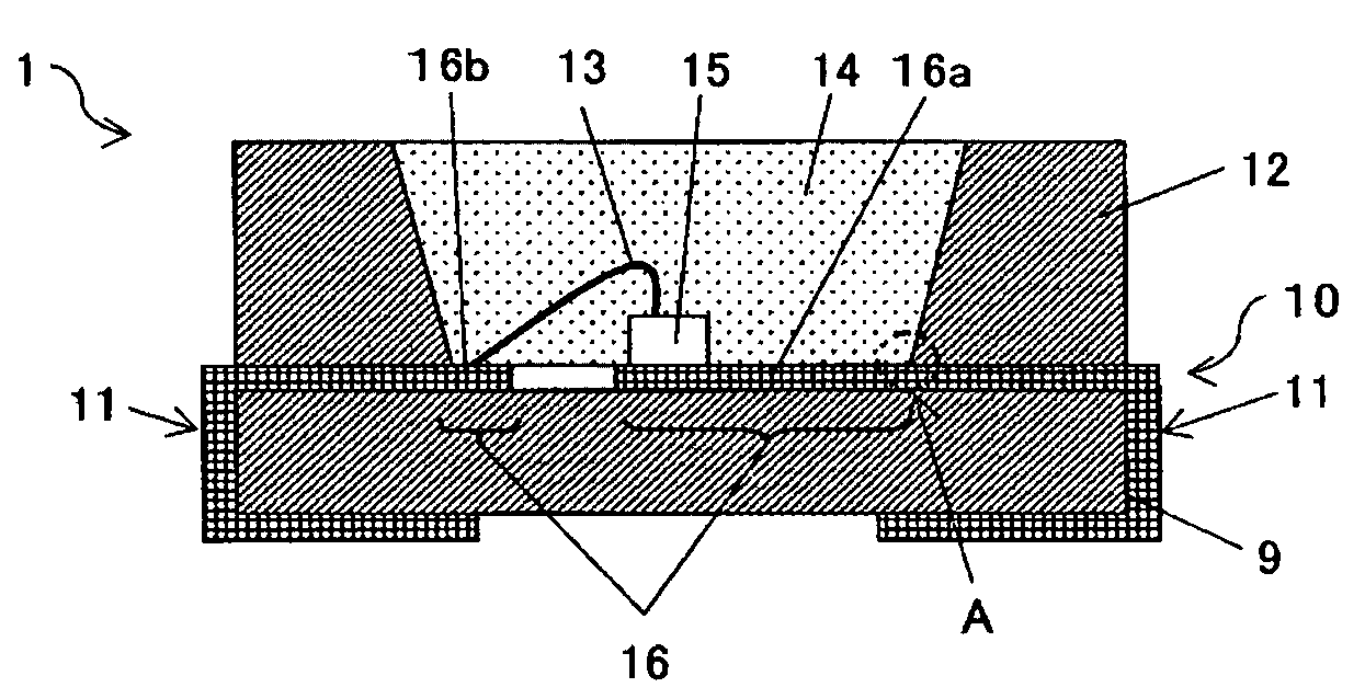
[0051]FIG. 1 is a schematic cross-sectional view of an optical semiconductor device pertaining to embodiment 1 of the present invention. FIG. 2 is a schematic cross-sectional view of a lead frame 10, showing an enlarged view of an area A of the optical semiconductor device 1. A dashed line B in FIG. 2 indicates a border between a feed lead area 16 and an external-connection lead area 11.

[0052]The optical semiconductor device 1 shown in FIG. 1 includes the lead frame 10, a peripheral resin 12, an Au wire 13 for electrical connection, a sealing resin 14, a light emitting element 15 and the like that are disposed on a substrate 9.

[0053]As shown in FIG. 2, the lead frame 10 has a basic structure in which a pure Ag plating layer 21 having a thickness of at least 1.5 μm has been formed on a surface of a plate-shaped metal base 20 that is composed of Cu, a Cu alloy, Fe, an Fe alloy etc., which have superior conductivity. Furthermore a plating lay...

embodiment 2

[0081]Structure

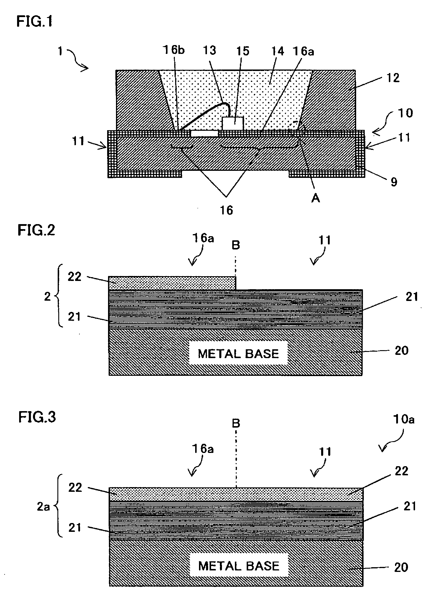
[0082]FIG. 3 is a schematic cross-sectional view showing a portion of a lead frame 10a of an optical semiconductor device pertaining to embodiment 2 of the present invention. The shown portion corresponds to an enlarged view of area A in FIG. 1.

[0083]A characteristic feature of the lead frame 10a is that a plating layer stack 2 is constituted from a pure Ag plating layer 21 and an Ag—Au alloy plating layer 22 that have been formed on an entire surface of one side of the lead frame 10a. The plating layers 21 and 22 have the same thicknesses as in embodiment 1.

[0084]This structure has the same effects as in embodiment 1, and the fact that the Ag—Au alloy plating layer 22 covers an entirety of one side of the lead frame 10a enables completely eliminating the danger of contact between the pure Ag plating layer 21 and the sealing resin 14, even if, for example, there are errors with respect to the disposed locations of the feed lead area 16 and the sealing resin 14. This s...

embodiment 3

[0088]Structure

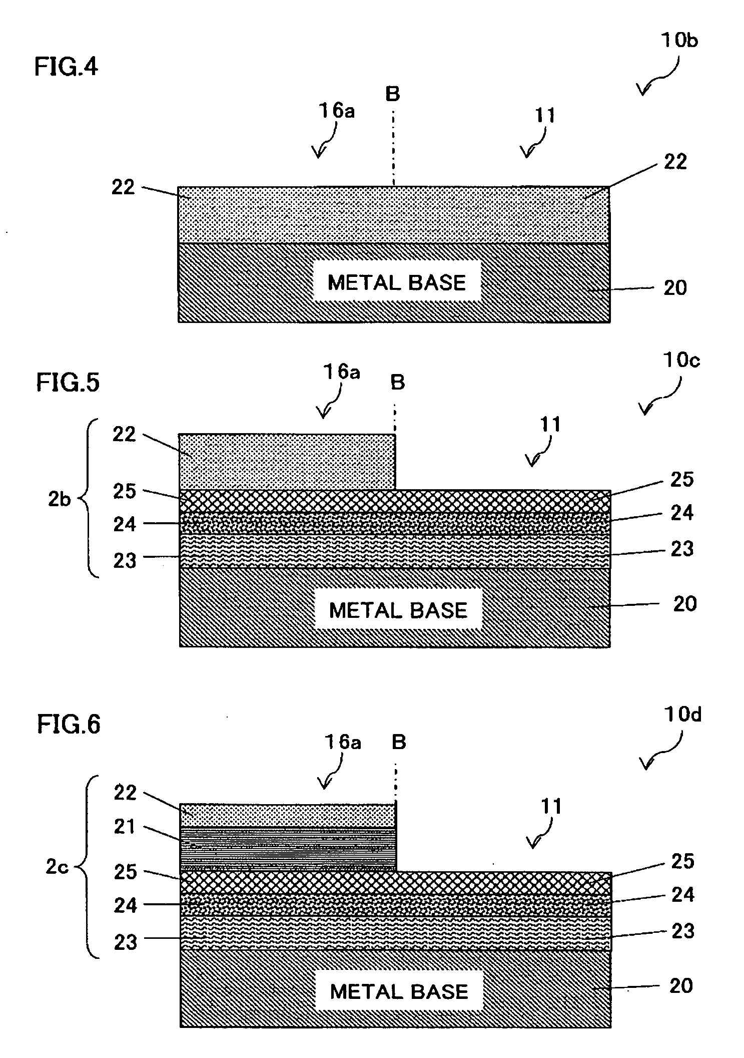
[0089]FIG. 4 is a schematic cross-sectional view showing a portion of a lead frame 10b of an optical semiconductor device pertaining to embodiment 3 of the present invention. The shown portion corresponds to an enlarged view of area A in FIG. 1.

[0090]A characteristic feature of the lead frame 10b is that the Ag—Au alloy plating layer 22 having a thickness of at least 1.5 μm has been formed directly on an entirety of one side of the metal base 20, and no pure Ag plating layer 21 has been provided. The plating method can be performed similarly to as in embodiment 2.

[0091]This structure has the same effects as embodiment 1, as well as effectively prevents contact between the pure Ag component and the sealing resin 14, even if, for example, there is partial peeling or damage to the Ag—Au alloy plating layer 22 in the feed lead area 16. This enables maintaining a superior luminous efficiency.


PUM

PropertyMeasurementUnit
thicknessaaaaaaaaaa
wavelengthaaaaaaaaaa
thicknessaaaaaaaaaa

Abstract

There is provided a lead frame for an optical semiconductor device, an optical semiconductor device using such lead frame, and a manufacturing method for these, where the optical semiconductor device exhibits favorable brightness over a long period of time by preventing discoloration and degeneration of a plating layer provide on the lead frame and a resulting reduction in a reflection coefficient for light emitted from a light emitting element, even when using silicone resin as a sealing resin. An Ag—Au alloy plating layer 22 is formed on the surface of a pure Ag plating layer 21 on a lead frame 10 sealed chloroplatinic acid-containing silicon resin, so as to prevent direct contact between the layer 21 and the silicone resin. This suppresses the formation of AgCl due to a reaction with a hardening catalyst of the silicon resin, thereby preventing the Ag plating layer from turning a blackish-brown color.

Description

BACKGROUND OF INVENTION[0001]1. Field of the Invention[0002]The present invention relates to a lead frame for an optical semiconductor device, and in particular to technology for preventing visual degradation of an optical semiconductor device in particular during emission of violet / blue light with a short wavelength (approximately 400 nm to 500 nm).[0003]2. Related Art[0004]Conventionally, optical semiconductor devices employing an LED element etc. as a light source are widely used as light sources in various types of display and illumination apparatuses.[0005]Such optical semiconductor devices include, for example, a lead frame disposed on a substrate, and a light emitting element mounted on the lead frame. Thereafter, the optical semiconductor device and a periphery thereof are sealed in a sealing resin in order to prevent degredation to the light source and surrounding region due to heat, humidity, oxidation, and the like.[0006]There is demand for the sealing resin material to h...

Claims


Application Information

Patent Timeline
Patent Type & Authority Applications(United States)
IPC IPC(8): H01L33/00H01L21/60H01R43/00H01L23/495H01L33/56H01L33/60H01L33/62
CPCH01L33/486Y10T29/49121H01L33/62H01L2224/48091H01L2224/48247H01L2924/01046H01L2924/01078H01L2924/01079H01L33/60H01L2224/48227H01L2224/45144H01L2924/01019H01L2924/00014H01L2924/00H01L2924/12044
Inventor YAMADA, TOMOYUKIFUTAGAMI, TOMOHIROKAWANO, KEISHIRO
Owner PANASONIC CORP
Why Eureka
Try Eureka