Manufacturing method of semiconductor device
- Summary
- Abstract
- Description
- Claims
- Application Information
AI Technical Summary
Benefits of technology
Problems solved by technology
Method used
Image

Examples
first embodiment
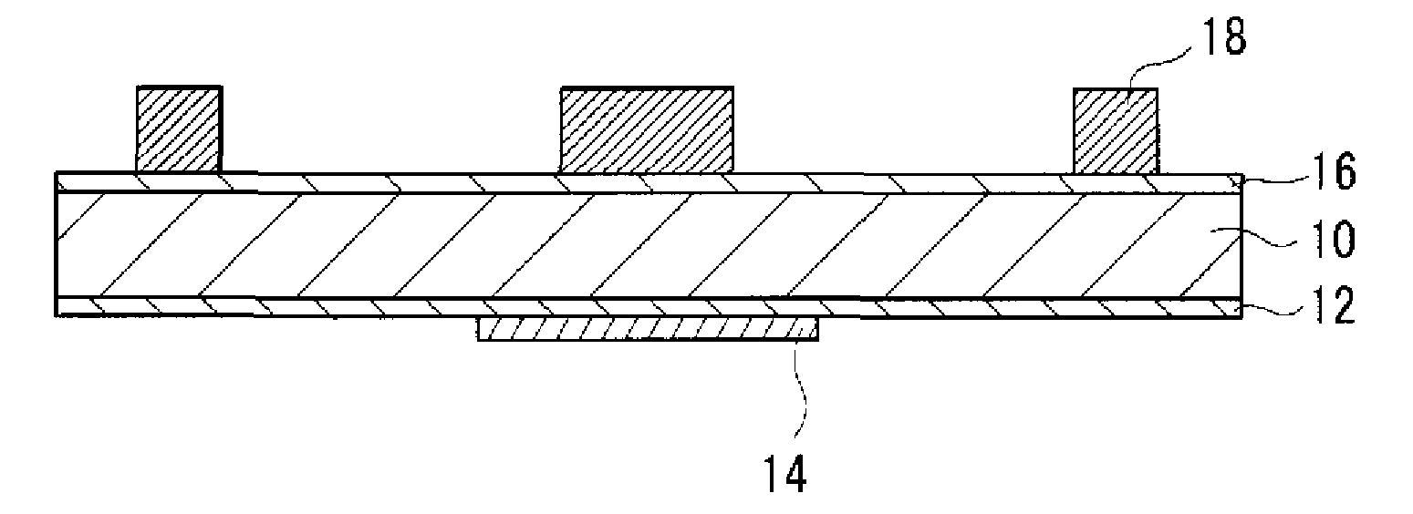
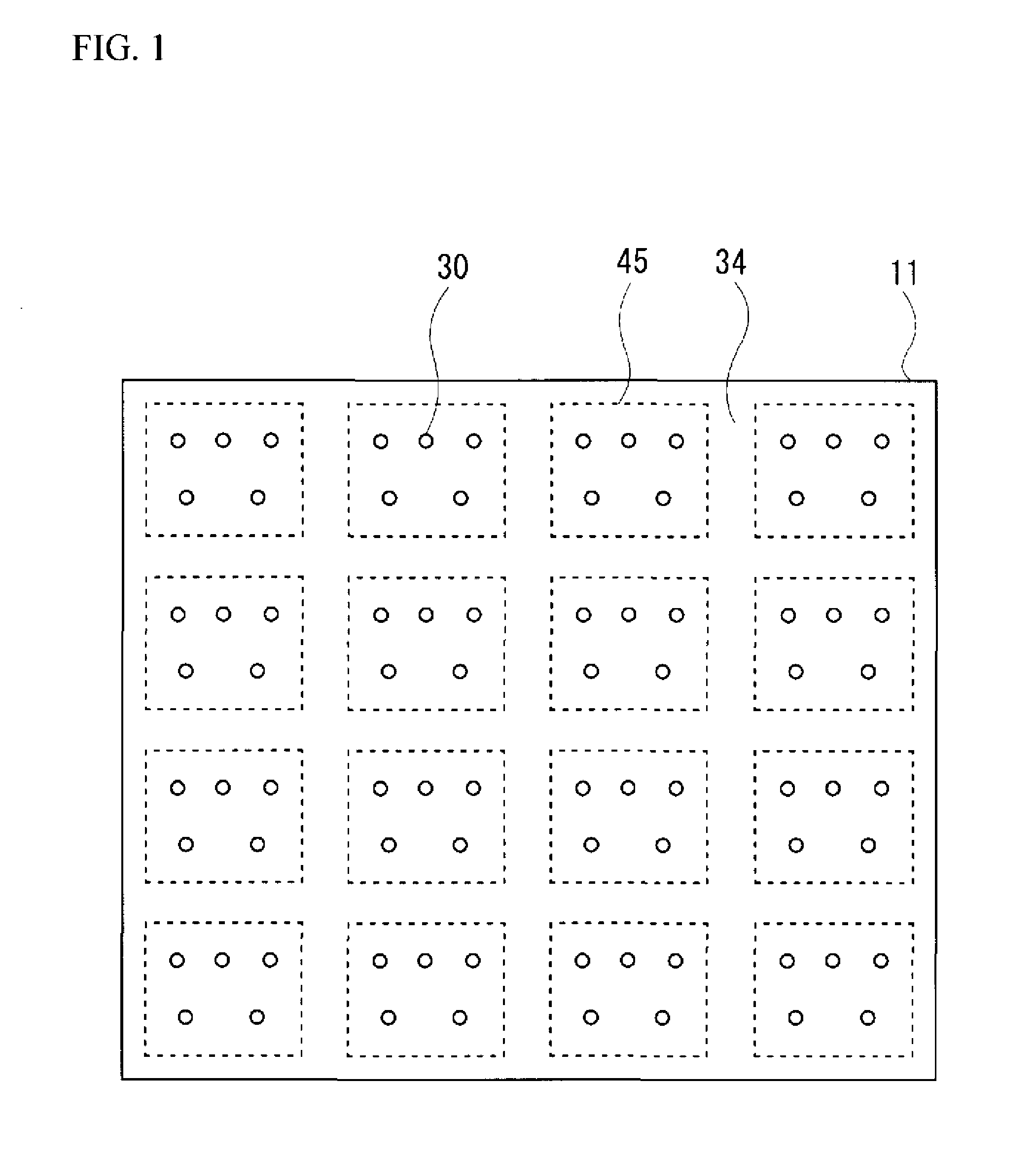
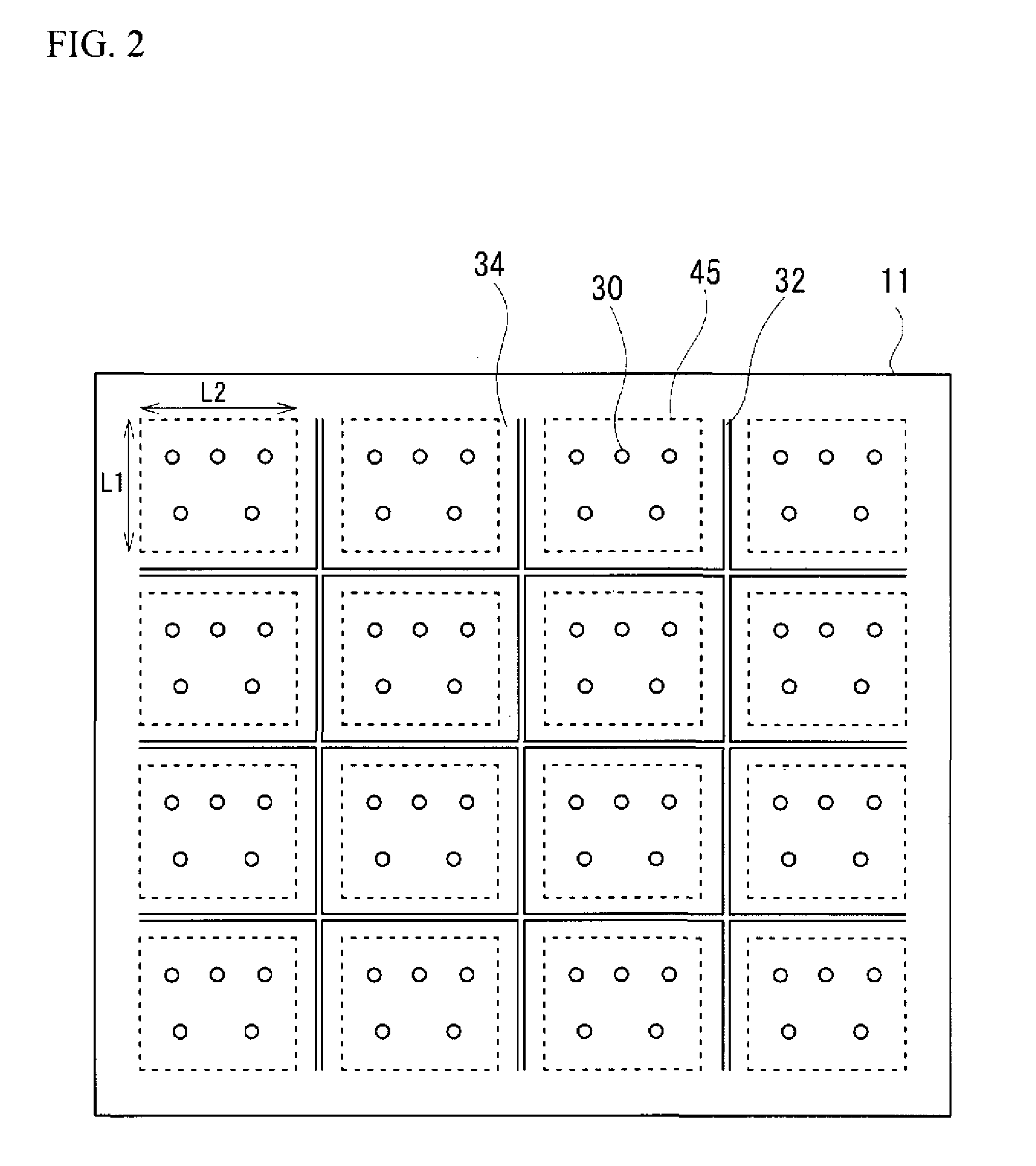
[0021] In a first embodiment, a metal mask composed of Ni or the like has a slit-shaped second open pattern 32 in the area 34 that is to be a scribe line, in addition to the first open pattern 30 for forming a through hole in a SiC substrate. FIG. 3A through FIG. 3D and FIG. 4A through FIG. 4C illustrate a cross sectional view showing a etching method of a SiC substrate in accordance with a first embodiment. The metal mask may be composed of Cu or the like having a large etching selectivity with respect to the substrate, in addition to Ni.
[0022] As shown in FIG. 3A, an epitaxial layer 12 composed of a GaN {gallium nitride}-based semiconductor layer or a SiC layer is formed on a front face (a face where an activation area or a circuit is formed) of a wafer-shaped SiC substrate 10. In FIG. 3A through FIG. 3D and FIG. 4A through FIG. 4C, the front face is illustrated down. An electrode pad 14 composed of Au is formed on a front face of the epitaxial layer 12. As shown in FIG. 3B, a fr...
second embodiment
[0036] A second embodiment is a case where the epitaxial layer 12 has an etching stopper layer 13. As shown in FIG. 8A, the epitaxial layer 12 has the stopper layer 13 and a GaN-based semiconductor layer 12a. The stopper layer 13 is, for example, composed of AlGaN. As shown in FIG. 8B, the SiC substrate 10 is subjected to an etching treatment with use of the metal mask 20 as a mask. It is possible to enlarge an etching selectivity of AlGaN with respect to GaN and SiC by changing a ratio of AlN in AlGaN suitably. Therefore, the etching is stopped at the stopper layer 13. The chips may be separated from each other if the epitaxial layer 12 of the recess 42 is removed. In accordance with the second embodiment, it is possible to remain the epitaxial layer 12 at the recess 42. It is therefore possible to restrain the separation of the chips. The stopper layer 13 may be provided on at least an area where the second open pattern is formed, and may be formed on an area where the first open ...
third embodiment
[0037] A third embodiment is a case where a GaN-based semiconductor layer 15 provided on a substrate is subjected to an etching treatment. As shown in FIG. 9, the GaN-based semiconductor layer 15 provided on the substrate 10 is subjected to a dry etching treatment with use of the metal mask 20 as a mask. And, patterns 40a and 42a are formed. A temperature of the substrate is increased because of a heat generated in an etching treatment if etching quantity is large, in a case where a layer provided on the substrate is subjected to the etching treatment. In accordance with the third embodiment, it is possible to restrain a generation of a crack caused by a thermal stress.
[0038] It may be at least one of the substrate 10 and a layer (the epitaxial layer 12 or the GaN-based semiconductor layer 15) provided on the substrate that are subjected to the dry etching treatment with use of the metal mask 20 as shown in the first through the third embodiments.
[0039] In the first through the th...
PUM
| Property | Measurement | Unit |
|---|---|---|
| Temperature | aaaaa | aaaaa |
| Area | aaaaa | aaaaa |
| Semiconductor properties | aaaaa | aaaaa |
Abstract
Description
Claims
Application Information
 - Generate Ideas
- Intellectual Property
- Life Sciences
- Materials
- Tech Scout
- Unparalleled Data Quality
- Higher Quality Content
- 60% Fewer Hallucinations
Browse by: Latest US Patents, China's latest patents, Technical Efficacy Thesaurus, Application Domain, Technology Topic, Popular Technical Reports.
© 2025 PatSnap. All rights reserved.Legal|Privacy policy|Modern Slavery Act Transparency Statement|Sitemap|About US| Contact US: help@patsnap.com