Attenuator

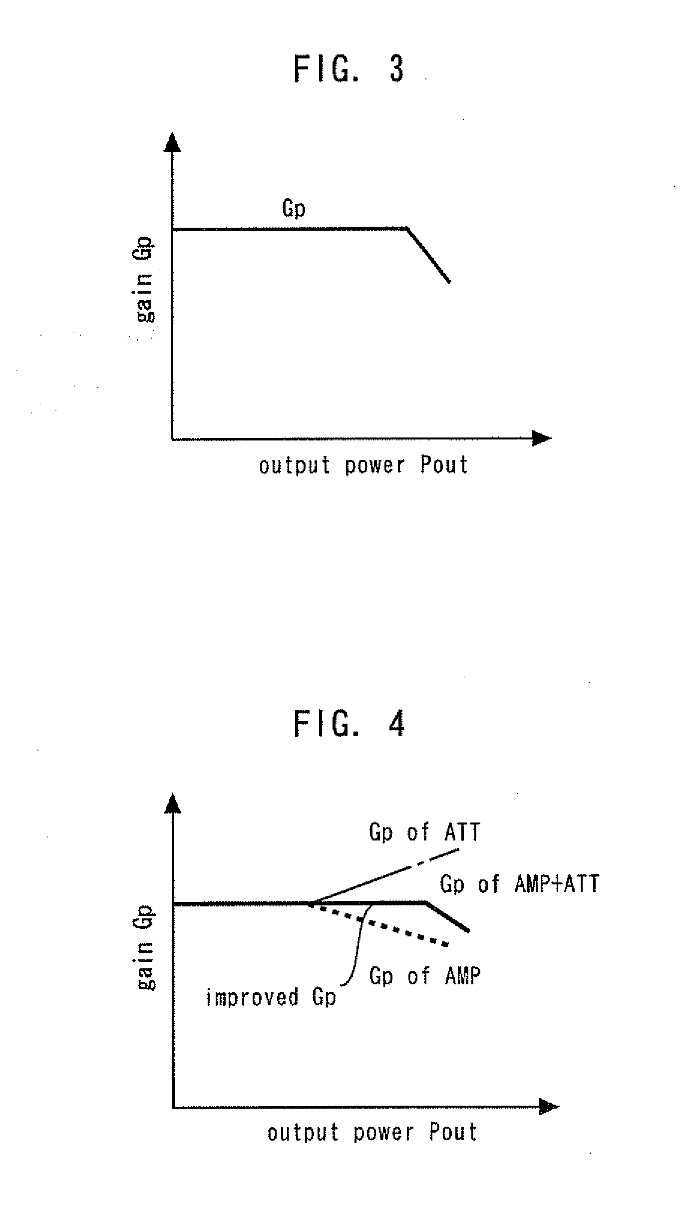
a diode attenuator and stacked type technology, applied in the direction of frequency-independent attenuators, automatic control of pulses, amplifiers, etc., can solve the problems of no degree of freedom in the structural design of the bc layer, and it is not possible to form a switch, so as to improve the characteristic of distortion, improve the flat section of the gain gp, and improve the characteristic of tertiary distortion pim3

Active Publication Date: 2008-04-17
MURATA MFG CO LTD
View PDF1 Cites 3 Cited by
  • Summary
  • Abstract
  • Description
  • Claims
  • Application Information

AI Technical Summary

Benefits of technology

[0025]FIG. 22 shows a characteristic at the time of attenuation of the attenuator in FIG. 21. The flat section of a gain Gp is improved as shown by a dotted line and the characteristic of tertiary distortion Pim3 is also improved accordingly. Therefore, this attenuator can improve the distortion characteristic at the time of high power input in the attenuation state, and therefore it is possible to tolerate a comparable degree of the distortion characteristic up to a comparable degree of transmit power in the thru state and the attenuation state. Furth

Problems solved by technology

However, when an RF (high frequency) switch element is constructed in a normal GaAs-HBT process, it is not possible to form a switch which can turn ON a channel only through application of a gate voltage.
Esp

Method used


Image

  • Attenuator
  • Attenuator
  • Attenuator

Examples


embodiment 1

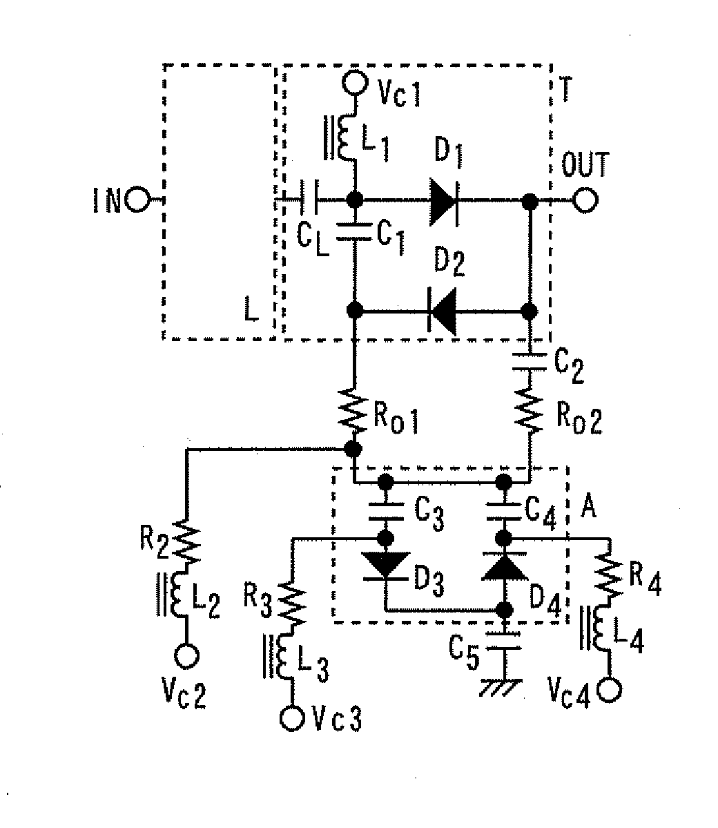
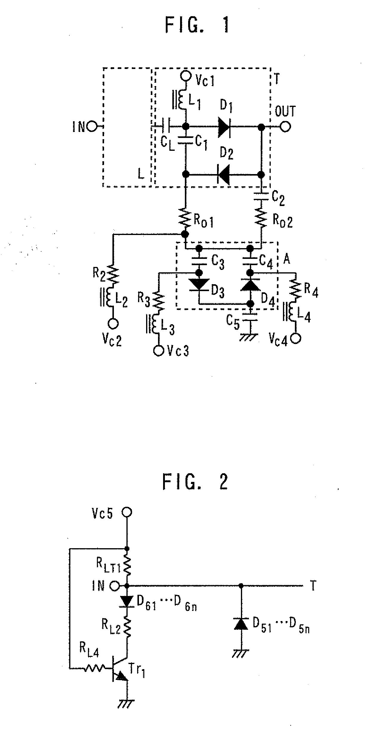
[0056]FIG. 1 is a circuit diagram showing an attenuator according to Embodiment 1 of the present invention. The anode of a diode D1 (first diode) is connected to an input terminal IN and the cathode of the diode D1 is connected to an output terminal OUT. Furthermore, a control voltage terminal Vc1 (first control voltage terminal) is connected to the anode of the diode D1 via an RF blocking inductor L1. The anode of a diode D2 (second diode) is connected to the cathode of the diode D1 and the cathode of the diode D2 is connected to the anode of the diode D1 via a capacitor C1 (first capacitor).

[0057]Furthermore, one end of a resistor R01 (first resistor) is connected to the cathode of the diode D2 and one end of a resistor R02 (second resistor) is connected to the cathode of the diode D1 via a capacitor C2 (second capacitor). The anode of a diode D3 (third diode) is connected to the other ends of the resistors R01 and R02 via a capacitor C3 (third capacitor) and the cathode of a diod...

embodiment 2

[0063]FIG. 5 is a circuit diagram showing a linearizer according to Embodiment 2 of the present invention. This linearizer L further includes a resistor RL3 (fourth resistor) whose one end is connected to a connection point of an input terminal IN and the anode of a D1 diode and a second n-channel MOS transistor Tr2 whose gate is connected to a control voltage terminal Vc6 (sixth control voltage terminal) via a resistor RL5, whose source is grounded and whose drain is connected to the other end of the resistor RL3. The rest of the configuration is the same as that in Embodiment 1.

[0064]Here, when a high-level voltage is applied to control voltage terminals Vc1, Vc4 and a low-level voltage is applied to control voltage terminals Vc2 and Vc3, a low-level voltage is applied to the control voltage terminal Vc6. This causes the second n-channel MOS transistor Tr2 to turn OFF. On the other hand, when a low-level voltage is applied to the control voltage terminals Vc1 and Vc4 and a high-le...

embodiment 3

[0066]FIG. 6 is a circuit diagram showing a linearizer according to Embodiment 3 of the present invention. This linearizer L further includes a diode D7 (seventh diode) whose anode is connected to a control voltage terminal Vc8 (eighth control voltage terminal) and a resistor RLA1 (seventh resistor) whose one end is connected to the cathode of the diode D7 and whose other end is connected to a connection point of an input terminal IN and the anode of a diode D1. The rest of the configuration is same as that in Embodiment 2.

[0067]While the diodes D51 to D5n operating in the attenuation state in Embodiments 1 and 2 are zero-biased, in this embodiment 3, a voltage (for example, 2 to 5 V) is applied to a control voltage terminal Vc8, and it is thereby possible to adjust the gain compression characteristic of the linearizer L to a desired characteristic. Other effects are the same as those in Embodiment 2.


PUM


Abstract

A linearizer includes fifth diodes, a third resistor, sixth diodes, and a first n-channel MOS transistor. When a low-level voltage is applied to first and fourth control voltage terminals and a high-level voltage is applied to second and third control voltage terminals, a low-level voltage is applied to a fifth control voltage terminal, and when a high-level voltage is applied to the first and fourth control voltage terminals and a low-level voltage is applied to the second and third control voltage terminals, a high-level voltage is applied to the fifth control voltage terminal.

Description

BACKGROUND OF THE INVENTION[0001]1. Field of the Invention[0002]The present invention relates to an AC-coupled, DC stacked type BC diode attenuator, and more particularly, to an attenuator capable of tolerating a comparable degree of a distortion characteristic up to a comparable degree of transmit power in a thru state and an attenuation state and an attenuator capable of compensating for a gain compression characteristic of a power amplifier in a thru state.[0003]2. Background Art[0004]A GaAs-HBT (hetero junction bipolar transistor) power amplifier is widely used as a power amplifier for a cellular phone carrying out CDMA (Code Division Multiple Access) or a power amplifier for a wireless LAN in recent years.[0005]Since the GaAs-HBT requires no negative gate bias voltage, it can operate with a single power supply and obtain a more uniform device characteristic than a GaAs-FET. Therefore, the GaAs-HBT has been increasingly applied to a GaAs-based power amplifier such as a cellular ...

Claims


Application Information

Patent Timeline
IPC IPC(8): H01P1/22H03H7/25H03H7/24
CPCH03F1/3276H03H11/24H03H7/253
Inventor YAMAMOTO, KAZUYAMIYASHITA, MIYO
Owner MURATA MFG CO LTD
Why Eureka
Try Eureka