Antenna component and methods

a technology of antenna and component, applied in the direction of simultaneous aerial operation, electrical apparatus, structural forms of radiation elements, etc., can solve the problems of antenna size, increase of losses, deterioration of efficiency,

Inactive Publication Date: 2008-04-17
PULSE FINLAND
View PDF9 Cites 79 Cited by
  • Summary
  • Abstract
  • Description
  • Claims
  • Application Information

AI Technical Summary

Benefits of technology

[0010] The invention has the advantage that an antenna component according to it is very small-sized. This is due to that the slot between the antenna elements is narrow and that the high permittivity of the substrate to be used. In addition, the invention has the advantage that the efficiency of an antenna made by a component according to it is good in spite of the dielectric substrate. A further advantage of the invention is that both the tuning and the matching of an antenna can be carried out without discrete components just by shaping the conductor pattern of the circuit board near the antenna component.
[0011] In another aspect of the invention, a device for use in an antenna apparatus is disclosed. In one embodiment, the device comprises: a dielectric substrate; a first conductive element positioned on the upper surface of the dielectric substrate; a second conductive element positioned on the upper surface of the dielectric substrate such that the second conductive element is separated from the first conductive element by a region; and at least one electrical contact point disposed on each of the first and second conductive elements.
[0012] In one variant, the region comprises a width of 0.5 mm or less.
[0013] In another variant, the dielectric substrate comprises a material selected from the group consisting of quartz, gallium-arsenide, and silicon.
[0014] In yet another variant, the area of the dielectric substrate is between 2 and 3 mm2, and the dielectric substrate comprises a thickness of 100 μm.
[0015] In a further variant, at least one of the first conductive element and the second conductive element comprise gold.

Problems solved by technology

However, such a reduction of the size of the antenna entails the increase of losses and thus a deterioration of efficiency.

Method used


Image

  • Antenna component and methods
  • Antenna component and methods
  • Antenna component and methods

Examples


Embodiment Construction

[0062]FIG. 1 was already explained in connection with the description of the prior art.

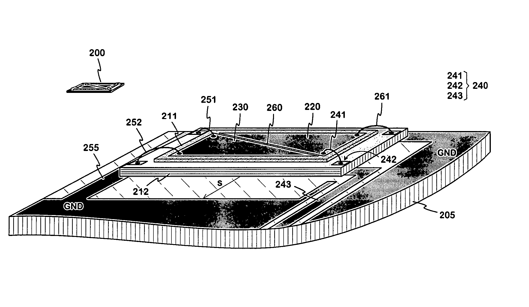
[0063]FIG. 2 shows an example of an antenna component and an whole antenna according to the invention. A part of the circuit board 205 of a radio device and an antenna component 200 on its surface are seen enlarged in the drawing. The antenna component 200 comprises a dielectric substrate 211 and two antenna elements on its surface, one of which has been connected to the antenna feed conductor and the other is an electromagnetically fed parasitic element, like in the antenna component 100 in FIG. 1. The difference is that the antenna elements now are located totally on the upper surface of the substrate, where their connection points then also are located. In the component of FIG. 1 the elements extend via the head surfaces to the lower surface of the substrate, where their connection points then also are, located. In addition, in the component according to the invention the slot 260 between the ...


PUM


Abstract

An antenna component (200) with a dielectric substrate and two radiating antenna elements. The elements are located on the upper surface of the substrate and there is a narrow slot (260) between them. The antenna feed conductor (241) is connected to the first antenna element (220), which is connected also to the ground by a short-circuit conductor (261). The second antenna element (230) is parasitic; it is galvanically connected only to the ground. The component is preferably manufactured by a semiconductor technique by growing a metal layer e.g. on a quartz substrate and removing a part of it so that the antenna elements remain. In this case the component further comprises supporting material (212) of the substrate chip. The antenna component is very small-sized because of the high dielectricity of the substrate to be used and mostly because the slot between the antenna elements is narrow. The efficiency of an antenna made by the component is high.

Description

PRIORITY AND RELATED APPLICATIONS [0001] This is a continuation application of and claims priority to International PCT Application No. PCT / FI2005 / 050401 having an international filing date of Nov. 8, 2005, which claims priority to PCT / FI2005 / 050247 having an international filing date of Jun. 28, 2005, and International PCT Application No. PCT / FI2005 / 050089 having an international filing date of Mar. 16, 2005, each of the foregoing incorporated herein by reference in its entirety. This application is related to co-owned and co-pending U.S. patent application Ser. No. 11 / 883,945 filed Aug. 6, 2007 entitled “Internal Monopole Antenna and Methods”; Ser. No. 11 / 801,894 filed May 11, 2007 and entitled “Antenna component and methods”; Ser. No. 11 / 544,173 filed Oct. 5, 2006 and entitled “Multi-Band Antenna With a Common Resonant Feed Structure and Methods”; Ser. No. 11 / 603,511 filed Nov. 22, 2006 and entitled “Multiband Antenna Apparatus and Methods”; Ser. No. 11 / 648,429 filed Dec. 28, 200...

Claims


Application Information

Patent Timeline
Patent Type & Authority Applications(United States)
IPC IPC(8): H01Q1/38H01Q9/04
CPCH01Q9/0407
Inventor SORVALA, JUHAANNAMAA, PETTERIKOSKINIEMI, KIMMO
Owner PULSE FINLAND
Why Eureka
Try Eureka