
Method And Apparatus For Evaluating Solar Cell And Use Thereof

a solar cell and output characteristic technology, applied in the field of methods, can solve the problems of high cost of solar cells made of si (silicon) or the like, impede the wide use of solar cells, and high cost of solar cells, and achieve the effect of reducing the cost of solar cells

Inactive Publication Date: 2008-04-17
NARA INSTITUTE OF SCIENCE AND TECHNOLOGY
View PDF6 Cites 34 Cited by
  • Summary
  • Abstract
  • Description
  • Claims
  • Application Information

AI Technical Summary

Benefits of technology

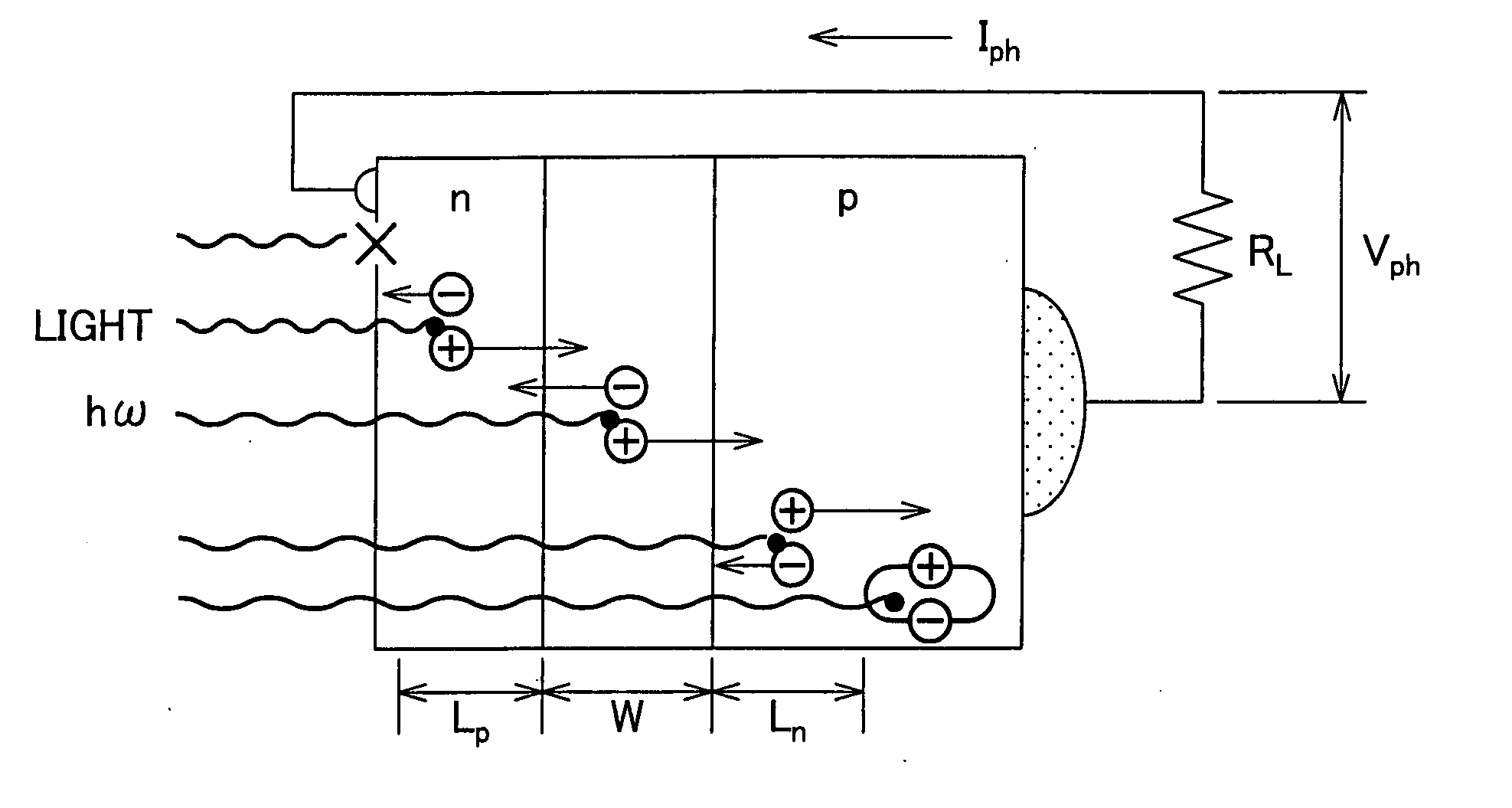
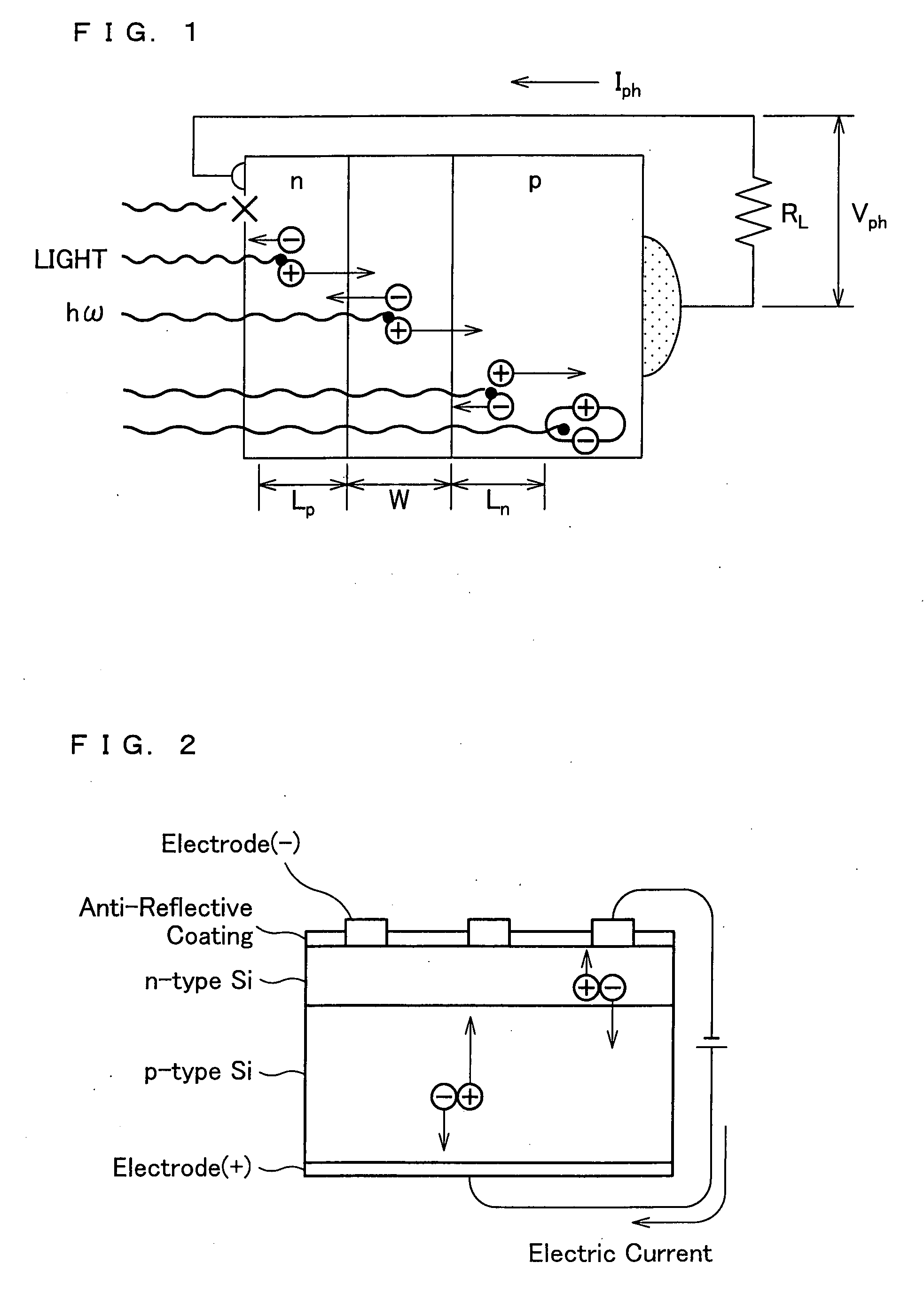
[0021] In view of the aforementioned problem, an object of the present invention is to provide a method and apparatus for evaluating a solar cell, which allow to evaluate a solar cell module in terms of its photoelectric conversion easily and accurately, without requiring a large-sized facility, and use thereof.
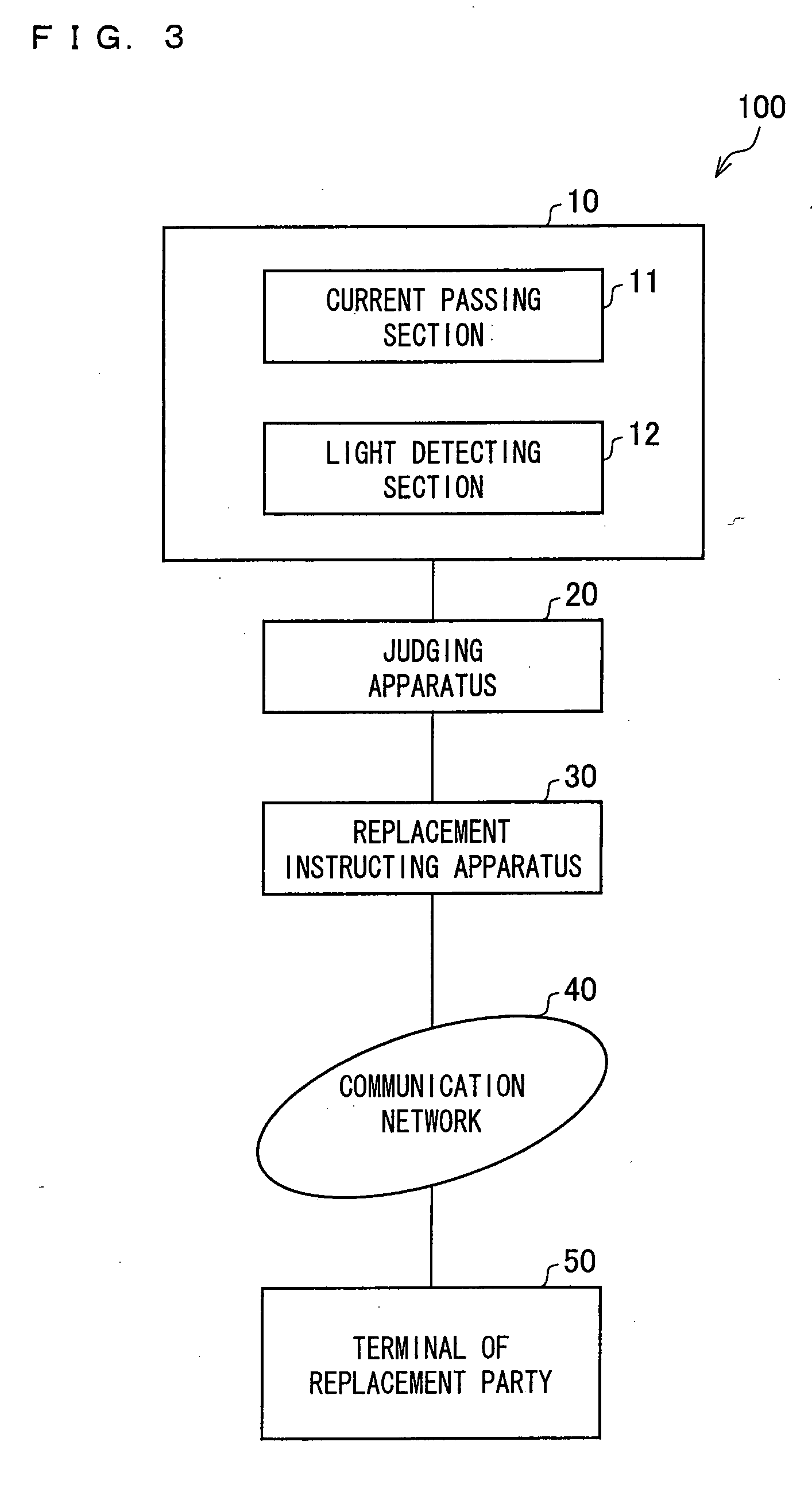
[0063] Furthermore, the method and apparatus of the present invention for evaluating the solar cell is advantageous over the conventional art, for example, in (i) it is not necessary to use a scanning probe (electron beam, laser), thus the measurement can be done easily, (ii) a large facility is not necessary, thus it is possible to observe and evaluate the solar cell as a product (as a product completed in the manufacturing factory or as a product implemented on a construction). Because of these and other advantages, it is also possible to establish a business model such as a maintenance method or a maintenance system in which a solar cell implemented on a construction is evaluated on a regular basis. The maintenance method and the maintenance system makes it possible to perform maintenance of the solar cell implemented on a construction, which has not been seldom carried out. Further, the maintenance method and the maintenance system make it possible to select a solar cell element whose performance is poor, instead of replacing the whole solar cell module. This attains high efficiency and low cost.

Problems solved by technology

Albeit solar cell modules including solar cell elements in which a plurality of solar cells are linked are implemented on more and more roofs or walls of ordinary buildings and houses, high cost of the solar cell made of Si (silicon) or the like hinders wide use of the solar cell.
One cause of the high cost of the solar cell is a need of a step of evaluating an output characteristics thereof regarding an output thereof made when sun light is irradiated on the solar cell module, that is a need of step of evaluating characteristics of the solar cell module.
In general, it is difficult to evaluate the output characteristics of the solar cell module by irradiating sun light directly on the solar cells, for example, because intensity of the sun light varies depending on weather.
The solar simulator and apparatuses for EBIC or LBIC are however, large in size and requires high equipment investment.
Moreover, there is such a problem that the evaluation methods using these apparatus are actually complicated.
That is, evaluation cost in the production cost of the solar cells has not been lowered due to high equipment cost of the measuring apparatuses for measuring and evaluating the performance of the solar cell element, and time-consuming measurement process.
This cannot perform such a detailed analysis to find out which solar cell element at which portion of the solar cell module has a poor conversion efficiency.
Furthermore, the apparatus for EBIC or LBIC has many facility restrictions such as a need of an electron microscope for radiating the electron beam, or a multi-wavelength light source for radiating the laser beam.
Therefore, it is not easy to perform this evaluation method for evaluating the solar cell module.
Therefore, silicon semiconductor has not been used as a light emitting material for LED or the like.
As described above, the light emitting characteristics of silicon semiconductor is not sufficient and silicon semiconductor is clearly different from GaAs in terms of its property.

Method used


Image

  • Method And Apparatus For Evaluating Solar Cell And Use Thereof
  • Method And Apparatus For Evaluating Solar Cell And Use Thereof
  • Method And Apparatus For Evaluating Solar Cell And Use Thereof

Examples


example

[0196] A Si solar cell element made from polycrystalline silicon semiconductor was analyzed by passing a forward current in a range of 5 to 40 mA / cm2. In the present Example, an emission microscope (Hamamatsu Photonics K.K. PHEMOS-200) was used. The Si solar cell element was 1 cm×1 cm in size. Images picturing the Si solar cell element through which the current was passed are illustrated in FIGS. 5(a) and 5(b). FIG. 5 (a) illustrates light emission from the Si solar cell element, while FIG. 5(b) illustrates a diffusion length of the minority carrier (electrons) in the Si solar cell element.

[0197]FIG. 5(a) shows that the Si solar cell element emitted strong light when the current passed therethrough. The whitish portion is a region where the light emission was strong, and the blackish portion is a region where the light emission was weak (in case of a color image, a reddish portion is the region where the light emission is strong, while a yellowish to bluish portion is the region wh...


PUM


Abstract

Disclosed is a method for evaluating the performance of a solar cell which comprises a silicon semiconductor as the main component. This method comprises a current introduction step for introducing a direct current into a solar cell element constituting the solar cell in the forward direction, and an emission sensing step for sensing emission characteristics of the light emitted from the solar cell element due to the current introduction step. By this method, the photoelectric conversion performance of a solar cell can be simply and accurately evaluated without requiring large-sized equipment.

Description

TECHNICAL FIELD [0001] The present invention relates to a method and apparatus for evaluating a solar cell easily and accurately in terms of a photoelectric conversion performance without using a large-sized detecting apparatus or the like, and use thereof. Especially, the present invention relates to a method and apparatus for evaluating a solar cell easily and accurately in terms of a photoelectric converting performance by passing an electric current through solar cell elements (e.g., a solar cell module, solar cell panel, or solar cell element per se) constituting the solar cell, and analyzing a light characteristics due to the electric current passage. BACKGROUND ART [0002] For keeping the environment of the earth, use of solar energy is getting popular. Albeit solar cell modules including solar cell elements in which a plurality of solar cells are linked are implemented on more and more roofs or walls of ordinary buildings and houses, high cost of the solar cell made of Si (si...

Claims


Application Information

Patent Timeline
Patent Type & Authority Applications(United States)
IPC IPC(8): G01J1/12
CPCG01J1/08G01J2001/4247G01N21/66H02S50/10Y02B10/12Y02E10/50H01L31/186Y02B10/10Y02P70/50
Inventor FUYUKI, TAKASHI
Owner NARA INSTITUTE OF SCIENCE AND TECHNOLOGY
Learn More