

Nanoimprint Mold, Method of Forming a Nonopattern, and a Resin-Molded Product
a nano-pattern and mold technology, applied in the field of nano-pattern forming molds, can solve the problems of mold durability decline, pattern breakage, and deterioration of releasability, and achieve the effects of reducing mold durability, reducing mold wear, and reducing mold wear
- Summary
- Abstract
- Description
- Claims
- Application Information
AI Technical Summary
Benefits of technology
Problems solved by technology
Method used
Image

Examples
embodiment 1
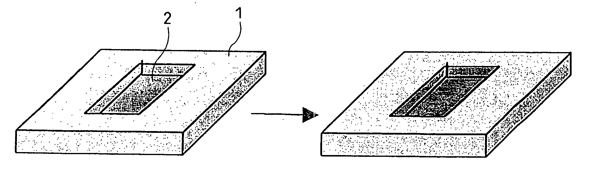
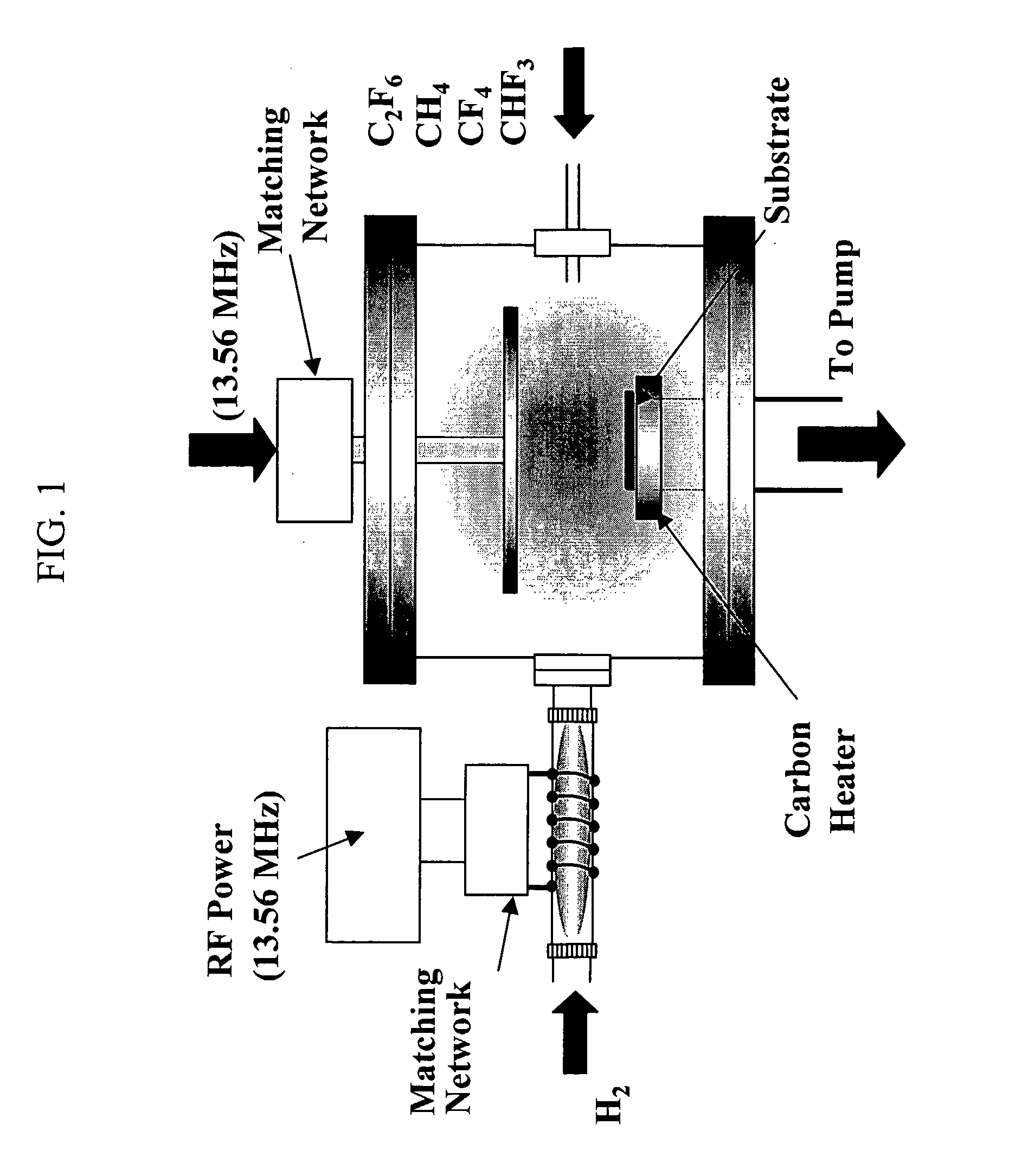
[0039] A mold structure with a CNW-patterned mold was prepared. In the present embodiment, the convex portions of the CNW correspond to the concave portions of a molded product. With reference to FIG. 6, a CNW was fabricated on a substrate for producing a CNW under the conditions described above with reference to a method of manufacturing a CNW (1). This was followed by the Ni-plating of the surface of the CNW (2). The plating process may involve substance other than Ni. Then, the CNW was peeled from the substrate (3). Alternatively, the CNW may be partly burned for removal. Finally, the CNW was fixed to the surface of the mold.
[0040] In the present embodiment, the white portions of the SEM image of the CNW correspond to the convex portions of the resin-molded product, as shown in the conceptual images in the drawing.
embodiment 2
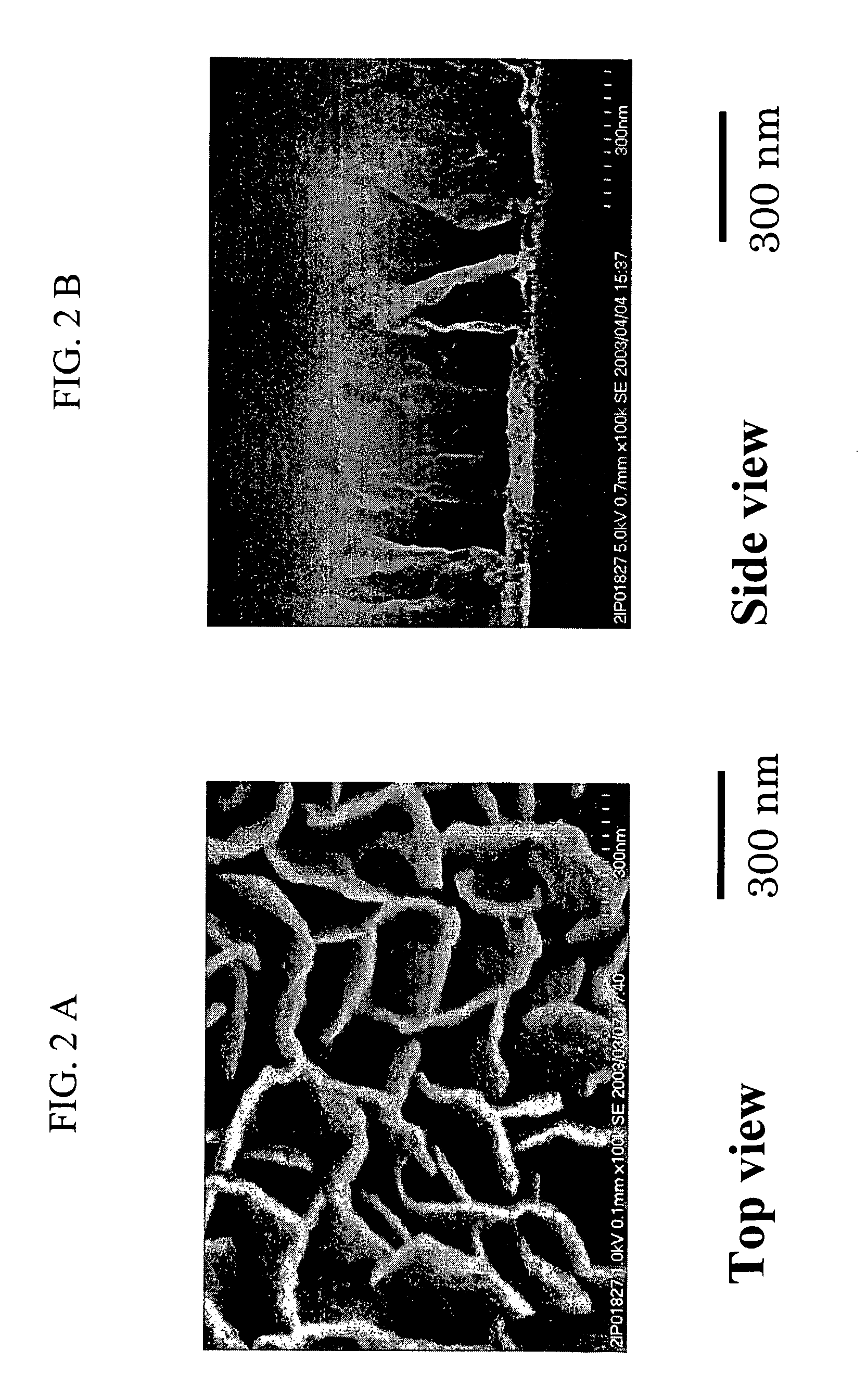
[0041] As shown schematically in FIG. 7, a mold structure with a reversed CNW-patterned mold was prepared. In the present embodiment, the convex portions of the CNW directly correspond to the convex portions of a molded product. Initially, a CNW was manufactured (1) on a substrate for producing a CNW under the conditions described with reference to the aforementioned method for forming a CNW. FIG. 8 shows an SEM image of the CNW surface prior to the Ni electroless plating process. Then, the surface of the CNW was provided with a Ni plating (2). FIG. 9 shows an SEM image of the CNW surface after the Ni electroless plating process. The plating process may involve a substance other than Ni. The CNW was then peeled from the substrate (3). FIG. 10 shows an SEM image of the surface on the CNW-removed side after the elimination of CNW by firing. It is seen from FIG. 10 that a reversed pattern of CNW is clearly present. The remaining CNW was burned at 700° C. in the air. Finally, the CNW wa...
PUM
| Property | Measurement | Unit |
|---|---|---|
| height | aaaaa | aaaaa |
| internal diameter | aaaaa | aaaaa |
| length | aaaaa | aaaaa |
Abstract
Description
Claims
Application Information