
Stacked chip package, embedded chip package and fabricating method thereof

a technology of embedded chips and chip packages, which is applied in the direction of semiconductor devices, electrical equipment, semiconductor/solid-state device details, etc., can solve the problems of uneven surface of dielectric materials, adversely affecting successive processes, and conventional semiconductor packaging technology is incapable of meeting the requirements of product functions and costs, etc., to reduce external electro-magnetic interference, reduce stress, and disperse the whole package

Active Publication Date: 2008-05-01
IND TECH RES INST
View PDF6 Cites 11 Cited by
  • Summary
  • Abstract
  • Description
  • Claims
  • Application Information

AI Technical Summary

Benefits of technology

[0010]The present invention provides a stacked chip package, an embedded chip package and fabricating method thereof, wherein various problems occurring in the conventional packaging schemes may be reduced. The fabrication method is compatible with the present semiconductor process. Thus, the process fabricating the embedded chip package can be simplified and the fabrication cost can be effectively reduced.
[0023]The present invention adopts an architecture, wherein an encapsulating material layer substitutes the core layer in the substrate of a conventional package. Thus, various disadvantages of the prior art described above effectively avoided. The encapsulating material layer can be used to support the semiconductor chip and the package's circuit layer and protect the semiconductor chip and the package. The material of the encapsulating material layer preferably comprises a coefficient of thermal expansion (CTE) close to that of the semiconductor chip's or has a capability of absorbing stress to reduce the stress caused by a CTE mismatch between different materials to the chip. The thermally / electrically conductive layer, e.g., a metal layer, in the architecture of the present invention is helpful to dissipate the whole package and reduce external electro-magnetic interference (EMI) or between the embedded and stacked chips. Contrary to the prior art, the architecture of the present invention allows integration of more number of chips in a single embedded chip package and thereby enhance the integration and efficiency of the device. On the other hand, bonding pads can be formed on two surfaces of the embedded chip package and can serve as a carrier for another package to form a stacked chip package. Thus, the cavity process of the prior art can be avoided. More particularly, the method of the present invention is compatible with the present semiconductor process and therefore the process is simple and effectively reduces the fabrication cost.

Problems solved by technology

In recent years, along with the update in tremendous pace for the electronic technology and the continuous integrations and renovations of the high-tech electronic products, the conventional semiconductor packaging technology is incapable of meeting the requirements of the product functions and cost.
However, the above-mentioned process methods are likely to make the surface of the dielectric material uneven to adversely affect the successive processes.
In particular, for a thicker chip, the thickness difference caused by the above-mentioned process methods would result in a poor surface evenness thereof and affect the production yield.
In order to solve the unevenness problem, it is very often to use a lapping process for thinning the chip or use more dielectric material to reduce the chip surface unevenness, and then the chip may be embedded, wherein the lapping processes may increase the fabrication cost and also may damage the chip during the chip embedded processes.
Thus, the fabrication cost may be further increased.
The disadvantage of the above scheme is that an additional filler is needed to fill the gaps between the chip and the substrate, the package thickness is mainly occupied by the thick substrate and the cavity depth is hard to control.
The disadvantage of this scheme is almost the same as the above described scheme where the package thickness is mainly occupied by the thick substrate, an additional filler is needed to fill the gaps between the chip and the substrate.
Thus, it is difficult to align the substrates.
Accordingly, how to embed a chip in a circuit substrate without encountering the problems described above is an important issue for the semiconductor manufacturers.

Method used


Image

  • Stacked chip package, embedded chip package and fabricating method thereof
  • Stacked chip package, embedded chip package and fabricating method thereof
  • Stacked chip package, embedded chip package and fabricating method thereof

Examples


first embodiment

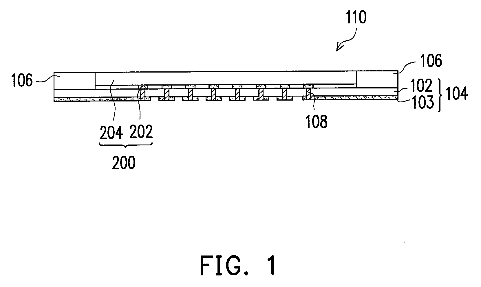
[0035]FIG. 1 is a cross-sectional drawing of the embedded chip package according to the present invention. The embedded chip package 110 of the embodiment mainly comprises a substrate 104, a semiconductor structure 200, an encapsulating material layer 106 and a plurality of conductive vias 108.

[0036]The substrate 104 herein mainly comprises a dielectric layer 102 and a patterned circuit layer 103 disposed on the dielectric layer 102. The material of the dielectric layer 102 is, for example, polyimide (PI), fiber reinforcement substrate (FR-4) / (FR-5), bismaleimide-triazine (BT), epoxy resin or other appropriate dielectric materials. The material of the patterned circuit layer 103 is, for example, a conductive material such as copper foil. The semiconductor structure 200 is disposed on the substrate 104. A plurality of electrical bonding pads 202 is disposed on the semiconductor structure 200 and contacts the dielectric layer 102. The material of the electrical bonding pads 202 is, fo...

second embodiment

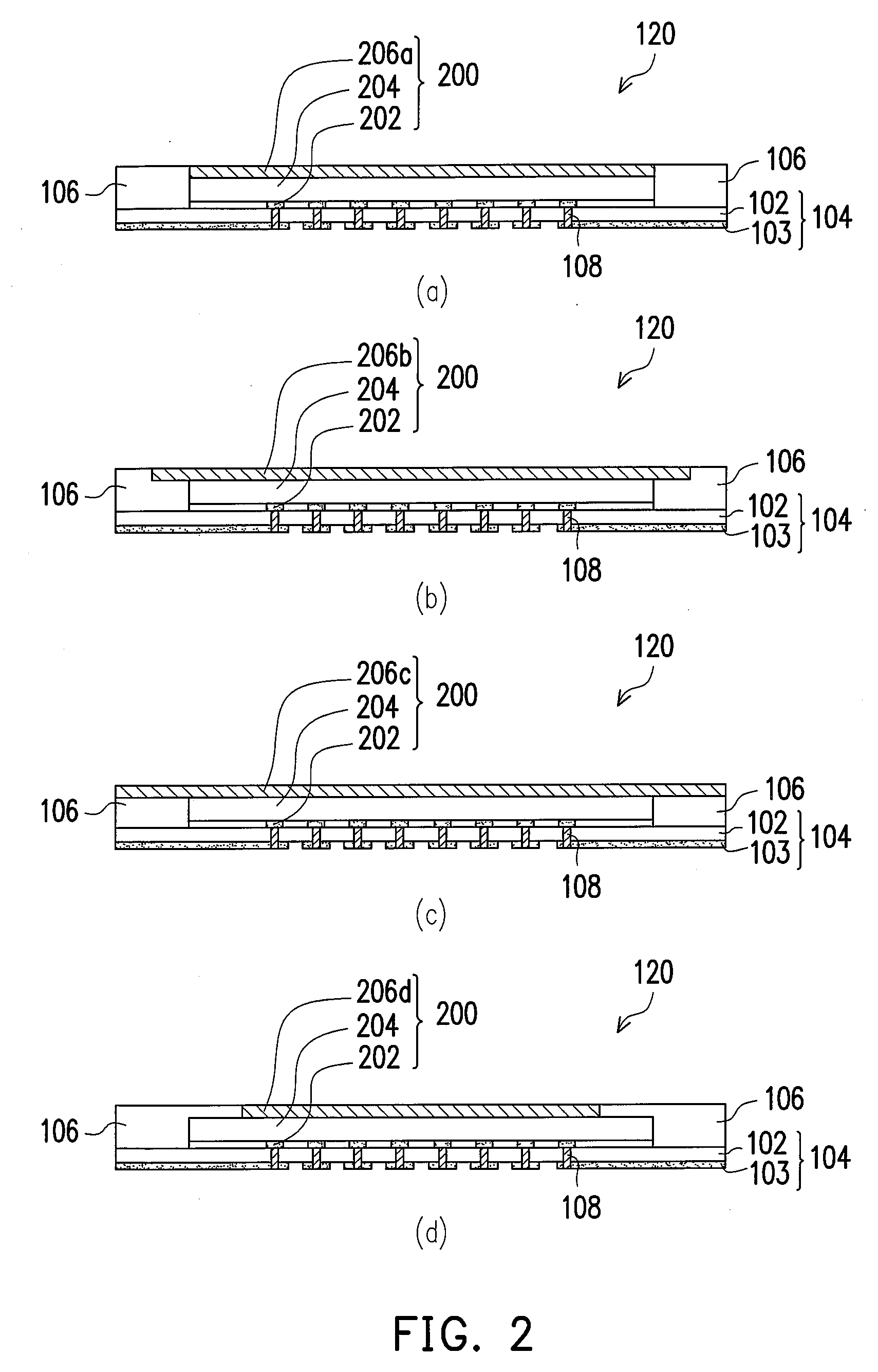
[0038]FIGS. 2(a)-2(d) are cross-sectional drawings of the embedded chip package according to the present invention. The embedded chip package 120 of the embodiment is similar to the embedded chip package 110 of the above-mentioned embodiment, except that the semiconductor structure 200 in the embedded chip package 120 further includes a cover layer 206a, 206b, 206c and 206d disposed on the semiconductor chip 204. The cover layer 206a may be disposed on the semiconductor chip 204 and the size of the cover layer 206a is equal to that of the semiconductor chip 204 as shown in FIG. 2(a). The cover layer 206b may be disposed on the semiconductor chip 204 and on a portion of the encapsulating material layer 106 as shown in FIG. 2(b). The cover layer 206c may be disposed on the semiconductor chip 204 and the encapsulating material layer 106 as shown in FIG. 2(c). The cover layer 206d may be disposed on the semiconductor chip 204 and the size of the cover layer 206d is smaller than that of ...

embodiment 3

[0039]FIGS. 3(a) and 3(b) are cross-sectional drawings of the embedded chip package corresponding to the present invention. The embedded chip package 130 of the embodiment is similar to the embedded chip package 110 of the above-mentioned embodiment, except that the semiconductor structure 200 in the embedded chip package 130 further includes a semiconductor chip 208 and a bonding layer 207. The semiconductor chip 208 is disposed over the semiconductor chip 204, a plurality of electrical bonding pads 210 is disposed on the upper surface of the semiconductor chip 208 and the lower surface thereof contacts the bonding layer 207. The material of the electrical bonding pads 210 is, for example, aluminum, copper, nickel / gold or other appropriate conductive materials. The bonding layer 207 is disposed between the semiconductor chip 204 and the semiconductor chip 208 and is comprised of an adhesive layer or a metal layer. FIG. 3(a) shows the structure of the embedded chip package 130 inclu...


PUM


Abstract

An embedded chip package includes a substrate, a semiconductor structure, an encapsulating material layer and a plurality of conductive vias. Herein the substrate includes at least a dielectric layer and at least a patterned circuit layer disposed on the dielectric layer. The semiconductor structure is disposed on the substrate and has a plurality of electrical bonding pads, and the electrical bonding pads contact the dielectric layer. The encapsulating material layer is disposed on the substrate and around the semiconductor structure. In addition, a plurality of conductive vias is disposed in the substrate to electrically connect the patterned circuit layer to the electrical bonding pads.

Description

CROSS-REFERENCE TO RELATED APPLICATION[0001]This application claims the priority benefit of Taiwan application serial no. 95140130, filed Oct. 31, 2006. All disclosure of the Taiwan application is incorporated herein by reference.BACKGROUND OF THE INVENTION[0002]1. Field of the Invention[0003]The present invention generally relates to a chip package and the fabricating method thereof, and more particularly, to a stacked chip package, an embedded chip package and a fabricating method thereof.[0004]2. Description of Related Art[0005]In the semiconductor industry, a chip packaging process is intended to avoid a bare chip from being affected by moisture, heat and noise and provide the bare chip with an electrical connection medium between the chip and the external circuit. In recent years, along with the update in tremendous pace for the electronic technology and the continuous integrations and renovations of the high-tech electronic products, the conventional semiconductor packaging te...

Claims


Application Information

Patent Timeline
Patent Type & Authority Applications(United States)
IPC IPC(8): H01L23/02H01L21/00
CPCH01L23/5389H01L24/18H01L2924/10253H01L24/82H01L2224/18H01L2224/82039H01L2924/01013H01L2924/01029H01L2924/01079H01L2924/01005H01L2924/01006H01L2924/01047H01L2924/01087H01L2924/014H01L2924/00H01L21/568H01L24/19H01L24/24H01L24/96H01L2224/04105H01L2224/73267H01L2924/181H01L2924/18162H01L2924/3025
Inventor SHEN, LI-CHENG
Owner IND TECH RES INST
Learn More