Amolded direct voltage pixel drive for minaturization

Inactive Publication Date: 2008-05-08
EMAGIN CORP
View PDF7 Cites 7 Cited by
  • Summary
  • Abstract
  • Description
  • Claims
  • Application Information

AI Technical Summary

Benefits of technology

[0016]In contrast to the NMOS source follower design illustrated in FIG. 1, the diode connected PMOS driver of the present invention operates to within one Vtp of the supply rail. Moreover, the present invention adds only one transistor to the basic NMOS source follower circuit, while still retaining an advantage of 20% fewer devices compared to the basic current driven cell. In addition, the voltage cell requires two fewer control lines for operation compared to the existing current cell design, further reducing complexity and size.
[0018]Although the PMOS drive transistor operates in the sub-threshold region, its operating point is not dependent on its gate to source voltage. Instead, the transistor is connected as a diode with its forward drop determined by the DATA voltage. The diode forward drop is set by programming a voltage onto the capacitor connected between the gate and drain, thus forming dynamically controlled voltage source. In this mode, the operating voltage for the OLED device is nearly proportional to the programming voltage signal. Small variations in the threshold voltage between PMOS drivers within the array result in only relatively minor differences between OLED voltages applied to the pixels, resulting in a good pixel to pixel uniformity even with minimum size transistors.
[0019]The maximum output voltage of the diode with this design is limited to one threshold below the positive rail. Since the drive transistor is a PMOS device, it is not subject to the body effect in a standard N-well semiconductor process. Also, the PMOS devices in the pixel array can be isolated from digital and other noise that is generated in the substrate by containing them in a separate N-well that is tied to a quiet voltage source, further improving low current and low light level performance in the microdisplay.
[0021]The benefit is a less expensive device with improved image quality that is required for large volume applications.

Problems solved by technology

However, with further scaling of the silicon process and reduced pixel sizes, it becomes more problematic to implement a current driven design due to area constraints, matching errors, and increased leakage currents.
A major drawback of that approach is that it suffers from a large body effect in a typical low-cost N-well semiconductor process.

Method used


Image

  • Amolded direct voltage pixel drive for minaturization
  • Amolded direct voltage pixel drive for minaturization
  • Amolded direct voltage pixel drive for minaturization

Examples


Embodiment Construction

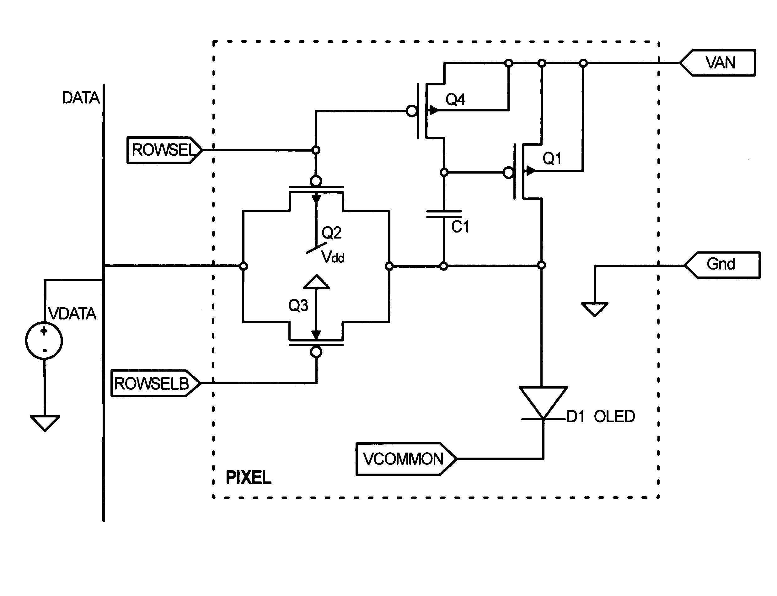
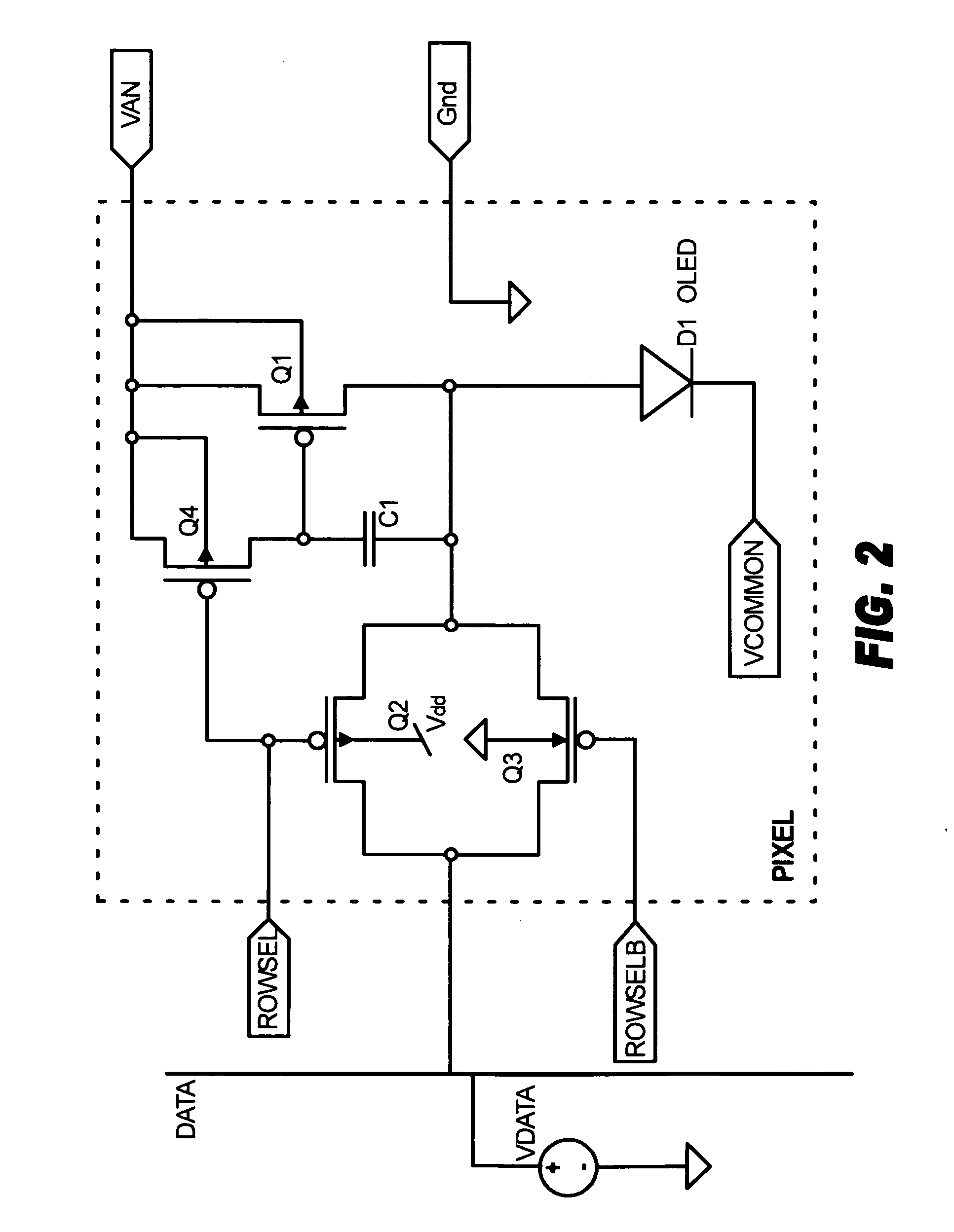
[0032]FIG. 2 shows a pixel driver that is based on a voltage source consisting of transistor Q1 and a storage capacitor C1. Transistor Q1 is configured as a MOS diode with the diode forward bias equal to the device threshold voltage plus the voltage across the capacitor C1. The current in the OLED is set by the voltage on the PMOS diode.

[0033]A CMOS transmission gate consisting of a transistor Q2 and a transistor Q3 acting as switches forms the data line access switch for the pixel. Both switches are closed by control signals ROWSEL and ROWSELB, respectively, during the programming phase in order to write data into the pixel. Both are opened at the end of the programming phase. In addition, the drain to substrate junction of transistor Q3 forms a clamp diode that protects the rest of the pixel circuitry from shorts across the OLED D1.

[0034]Transistor Q4 is used to preset one side of the storage capacitor to a fixed reference voltage during the pixel programming phase, eliminating pi...


PUM


Abstract

The drive circuit for an OLED is designed for use with an external reference voltage source. The OLED is connected to the reference voltage source through a PMOS drive transistor. The circuit includes a data signal transmission gate responsive to a control signal for transmitting the data signal to the OLED. It also includes a storage capacitor and a second transistor. The capacitor is connected between the gate and the source of the drive transistor. The second transistor has an output circuit connected between the reference voltage source and the capacitor. The gate of the second transistor is operably connected to receive the control signal.

Description

CROSS-REFERENCE TO RELATED APPLICATIONS[0001]Not ApplicableSTATEMENT REGARDING FEDERALLY SPONSORED RESEARCH OR DEVELOPMENT[0002]Not ApplicableREFERENCE TO A “SEQUENCE LISTING”, A TABLE, OR A COMPUTER PROGRAM LISTING APPENDIX SUBMITTED ON COMPACT DISC[0003]Not ApplicableBACKGROUND OF THE INVENTION[0004]1. Field of the Invention[0005]The present invention relates to pixel driver circuits for active matrix organic light emitting diode (AMOLED) displays and microdisplays and, more particularly, to such a circuit that permits further reduction of the size of the pixel while maintaining good pixel uniformity and performance.[0006]2. Description of Prior Art Including Information Disclosed Under 37 CFR 1.97 and 1.98[0007]There are many publications, for example those published in the SID Symposium Proceedings 2001 through 2004 that relate to overcoming the problem of threshold voltage variation for poly and amorphous silicon based direct view AMOLED displays. I am also aware of several pat...

Claims


Application Information

Patent Timeline
IPC IPC(8): G09G3/30
CPCG09G3/3258G09G2300/0842G09G2300/0465
Inventor WACYK, IHOR
Owner EMAGIN CORP
Why Eureka
Try Eureka