Plasma etching apparatus and method

a technology of plasma etching and apparatus, which is applied in the direction of electrical equipment, decorative arts, electrical discharge tubes, etc., can solve the problems of difficult to etch the sioc family low-k film with a high selectivity and a high etching rate, and achieve high etching rate and high selectivity

Active Publication Date: 2008-05-15
TOKYO ELECTRON LTD
View PDF5 Cites 79 Cited by
  • Summary
  • Abstract
  • Description
  • Claims
  • Application Information

AI Technical Summary

Benefits of technology

[0016]An object of the present invention is to provide a plasma etching apparatus and plasma etching method, which can etch an etching target film with a high selectivity and a high etching rate.
[0017]Another object of the present invention is to provide a plasma etching apparatus and plasma etching method, which can suppress the micro-loading effect.

Problems solved by technology

In general, a mixture gas based on a fluorocarbon gas is used as a process gas to provide a relatively high selectivity of a target film relative to an underlying film, but this is not enough to ensure a sufficient selectivity.
In this case, however, the margin for ensuring a sufficient etching selectivity between the film and layer is narrow and makes it difficult to etch the SiOC family Low-k film with a high selectivity and a high etching rate.
On the other hand, where etching of via holes or contact holes is performed in a parallel-plate plasma etching apparatus of the capacitive coupling type, a so-called micro-loading effect is undesirably caused, such that the etching rate varies depending on the size of holes, and makes it difficult to control the etching depth.
Where no etching-stopper layer is disposed, the etching depth fluctuates due to the micro-loading effect, and carries over the fluctuations to subsequent steps, thereby deteriorating the uniformity of electric properties.
Even where an etching-stopper layer is disposed, an over etching time needs to be prolonged, and thus brings about additional losses and fluctuations on the underlying layers, which adversely affect electric properties.
However, with decreases in the pressure and flow rate during a process, the selectivity relative to a mask and / or an underlying layer becomes smaller, thereby deteriorating the flexibility of the process.

Method used


Image

  • Plasma etching apparatus and method
  • Plasma etching apparatus and method
  • Plasma etching apparatus and method

Examples


first embodiment

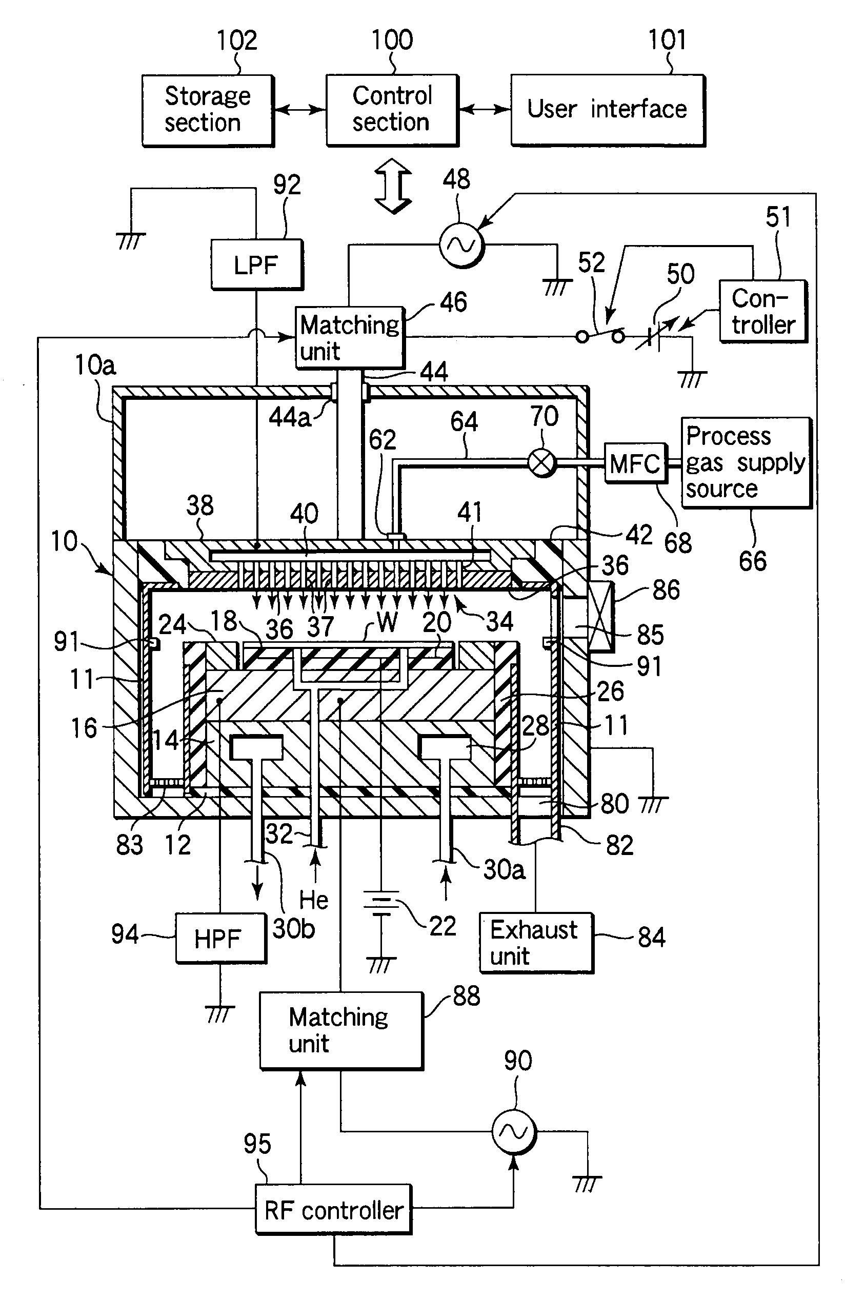
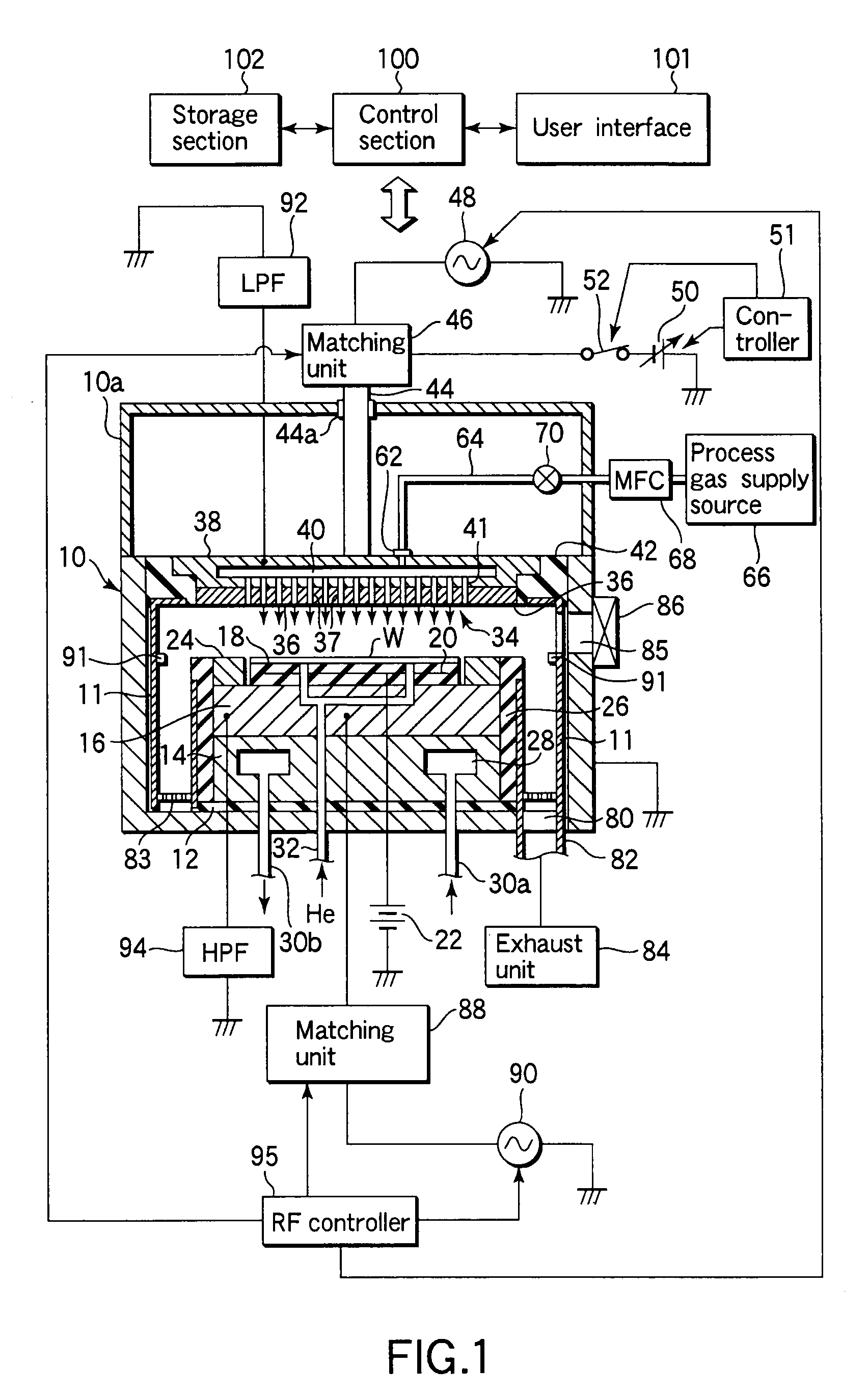
[0063]At first, an explanation will be given of the present invention.

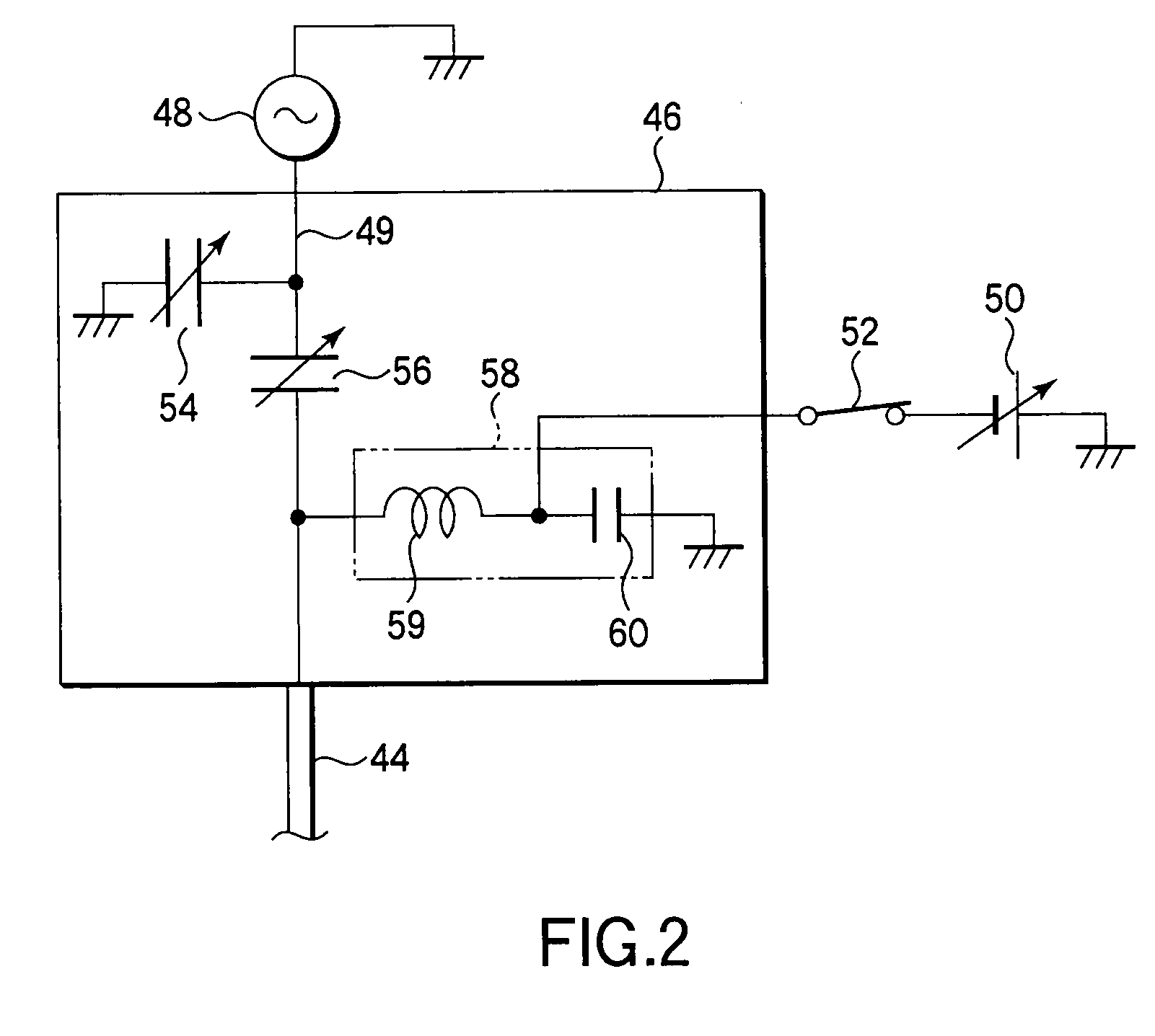
[0064]FIG. 1 is a sectional view schematically showing a plasma etching apparatus according to the first embodiment of the present invention.

[0065]This plasma etching apparatus is structured as a parallel-plate plasma etching apparatus of the capacitive coupling type. The apparatus includes an essentially cylindrical chamber (process container) 10, which is made of, e.g., aluminum with an anodization-processed surface. The chamber 10 is protectively grounded.

[0066]A columnar susceptor pedestal 14 is disposed on the bottom of the chamber 10 through an insulating plate 12 made of, e.g., a ceramic. A susceptor 16 made of, e.g., aluminum is disposed on the susceptor pedestal 14. The susceptor 16 is used as a lower electrode, on which a target substrate, such as a semiconductor wafer W, is placed.

[0067]The susceptor 16 is provided with an electrostatic chuck 18 on the top, for holding the semiconductor wafer W by an el...

second embodiment

[0176]Next, an explanation will be given of the present invention.

[0177]FIG. 20 is a sectional view schematically showing a plasma etching apparatus according to a second embodiment of the present invention.

[0178]This plasma etching apparatus has a structure essentially the same as that of the plasma etching apparatus according to the first embodiment except that an RF power for plasma generation is applied to the lower electrode or susceptor. Accordingly, the same constituent elements as those in FIG. 1 are denoted by the same reference numerals in FIG. 20, and their description will be omitted.

[0179]In this embodiment, a lower electrode or susceptor 16 is connected to both of a first RF power supply 48′ for plasma generation and a second RF power supply 90 for applying a bias for ion attraction. The first RF power supply 48′ is connected to the susceptor 16 through a first matching unit 89. The first matching unit 89 has the same structure as the second matching unit 88, and, when...


PUM

PropertyMeasurementUnit
frequencyaaaaaaaaaa
frequencyaaaaaaaaaa
poweraaaaaaaaaa

Abstract

An upper electrode and a lower electrode are disposed opposite to each other in a process container configured to be vacuum-exhausted. The upper electrode is connected to a first RF power supply configured to apply a first RF power for plasma generation. The lower electrode is connected to a second RF power supply configured to apply a second RF power for ion attraction. The second RF power supply is provided with a controller preset to control the second RF power supply to operate in a power modulation mode that executes power modulation in predetermined cycles between a first power set to deposit polymers on a predetermined film on a wafer and a second power set to promote etching of the predetermined film on the wafer.

Description

BACKGROUND OF THE INVENTION[0001]1. Field of the Invention[0002]The present invention relates to a plasma etching apparatus, plasma etching method, and computer readable storage medium, used for performing a plasma etching on a target substrate, such as a semiconductor substrate.[0003]2. Description of the Related Art[0004]For example, in the process of manufacturing semiconductor devices, plasma etching processes, which utilize plasma to etch a layer through a resist mask, are often used for forming a predetermined pattern on a predetermined layer disposed on a target substrate, such as a semiconductor wafer.[0005]Although various plasma etching apparatuses for performing such plasma etching are present, parallel-plate plasma etching apparatuses of the capacitive coupling type are in the mainstream of them.[0006]In general, a parallel-plate plasma etching apparatus of the capacitive coupling type includes a chamber with a pair of parallel-plate electrodes (upper and lower electrode...

Claims


Application Information

Patent Timeline
Patent Type & Authority Applications(United States)
IPC IPC(8): C23F1/02C23F1/08
CPCH01J2237/334H01J37/32027H01L21/30655H01J2237/3346H01L21/76802H01L21/31116H01J37/32091H01L21/76834H01J37/32183H01J37/32137H01J37/32165H01J37/32174H01L21/3065
Inventor KOSHIISHI, AKIRAKOBAYASHI, NORIYUKIYONEDA, SHIGERUHANAWA, KENICHITAHARA, SHIGERUSUGIMOTO, MASARU
Owner TOKYO ELECTRON LTD
Why Eureka
Try Eureka