Switched capacitor circuit with inverting amplifier and offset unit
- Summary
- Abstract
- Description
- Claims
- Application Information
AI Technical Summary
Benefits of technology
Problems solved by technology
Method used
Image
Examples
Embodiment Construction
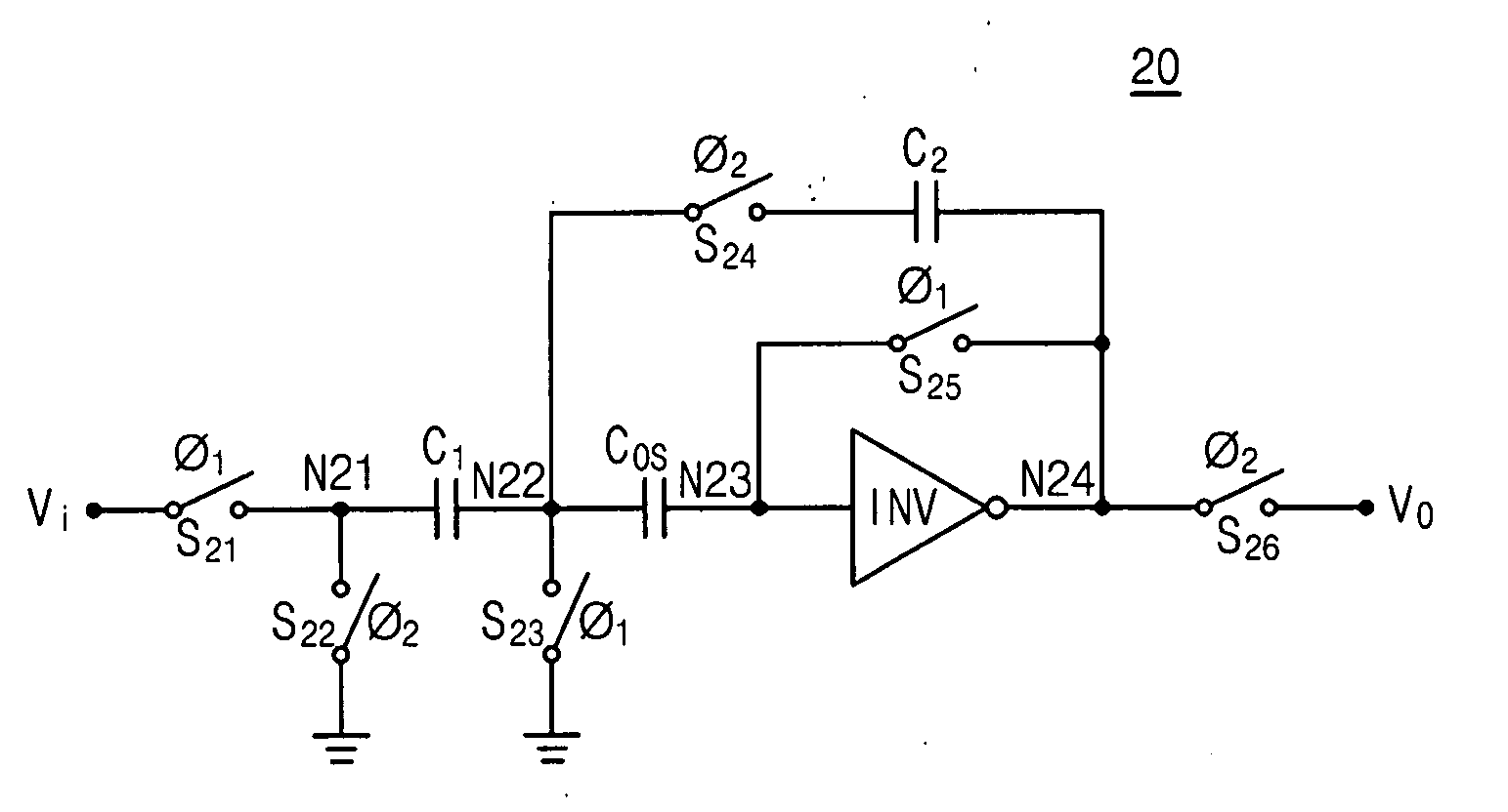
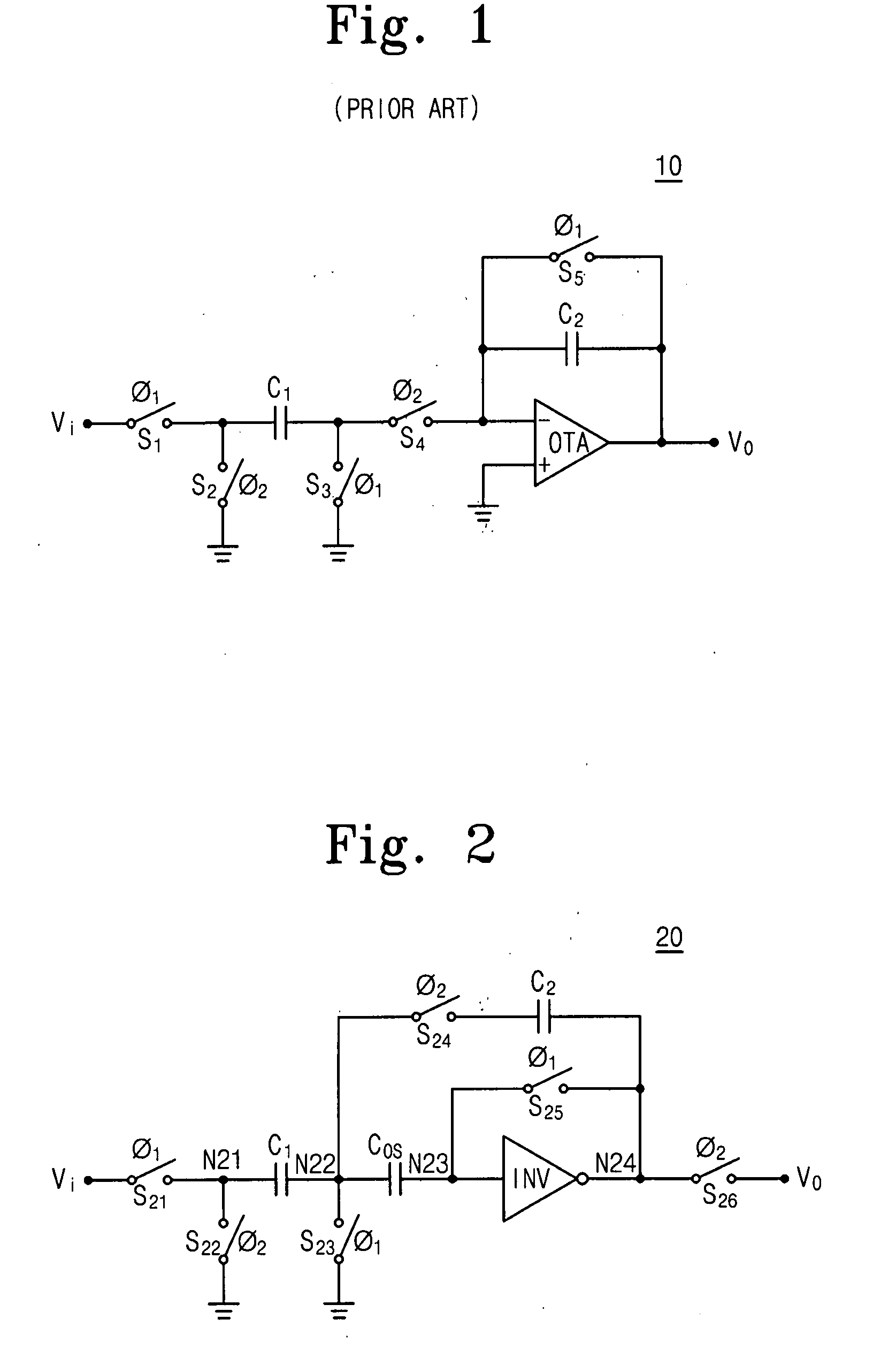
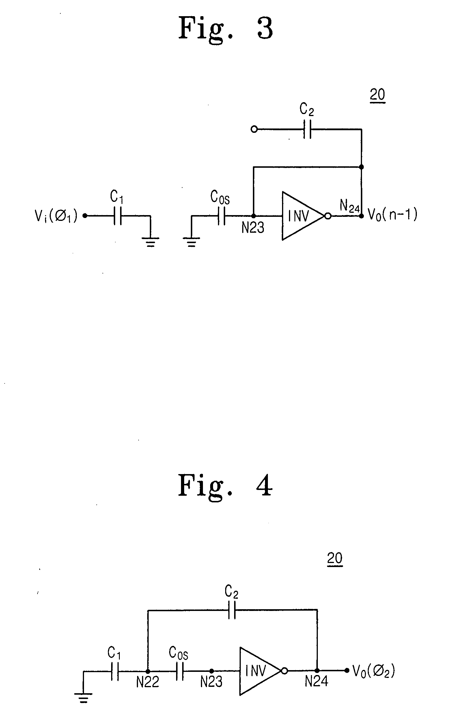
[0039]FIG. 2 shows a switched capacitor circuit 20 for implementing an integrator according to an embodiment of the present invention. Referring to FIG. 2, the switched capacitor circuit 20 includes an inverter INV, and first, second, third, fourth, fifth, and sixth switches S21, S22, S23, S24, S25, and S26, respectively. The switched capacitor circuit 20 also includes a sampling capacitor C1, an offset capacitor Cos, and a feedback capacitor C2.
[0040]The inverter INV is single-ended with a single input and a single output according to an embodiment of the present invention. Such an inverter has a simpler circuitry than the OTA of the prior art such that the switched capacitor circuit 20 consumes less power and occupies less integrated circuit area. The inverter INV is a typical inverter having a gain of about −1 in one embodiment of the present invention. Alternatively, the inverter INV is an inverting amplifier providing a negative gain with a magnitude of the gain being greater t...
PUM
 Abstract
Description
Claims
Application Information


