Dynamic surface annealing using addressable laser array with pyrometry feedback

a laser array and dynamic surface technology, applied in the field of thermal processing of semiconductor substrates, can solve the problems of short time that the wafer needs to stay at the highest temperature, cannot avoid heating the entire bulk of the wafer, and the annealing time must be limited

Active Publication Date: 2008-05-29
APPLIED MATERIALS INC
View PDF9 Cites 320 Cited by
  • Summary
  • Abstract
  • Description
  • Claims
  • Application Information

AI Technical Summary

Problems solved by technology

The time that the wafer needs to stay at the highest temperature can be very short.
Such lamps have an on / off switching time of at least a half second and therefore cannot avoid heating the entire bulk of the wafer.
As a result, the anneal time must be limited to avoid exceeding the thermal budget.
Such pyrometers are generally inappropriate for the focused laser beams of DSA apparatus the irradiate only a small area of the wafer at any time, leaving the bulk of the wafer near ambient temperature.

Method used


Image

  • Dynamic surface annealing using addressable laser array with pyrometry feedback
  • Dynamic surface annealing using addressable laser array with pyrometry feedback
  • Dynamic surface annealing using addressable laser array with pyrometry feedback

Examples


Embodiment Construction

Introduction:

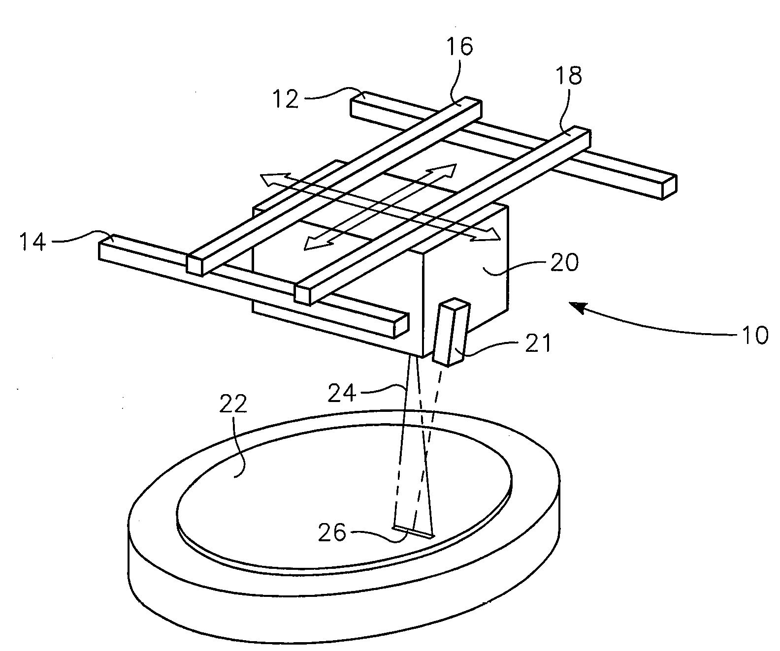
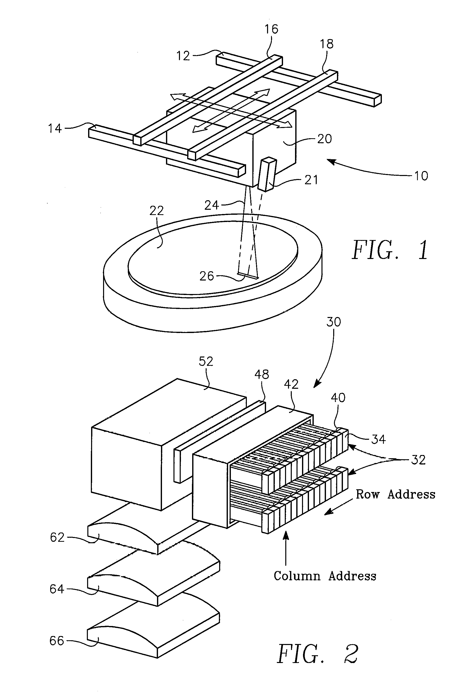
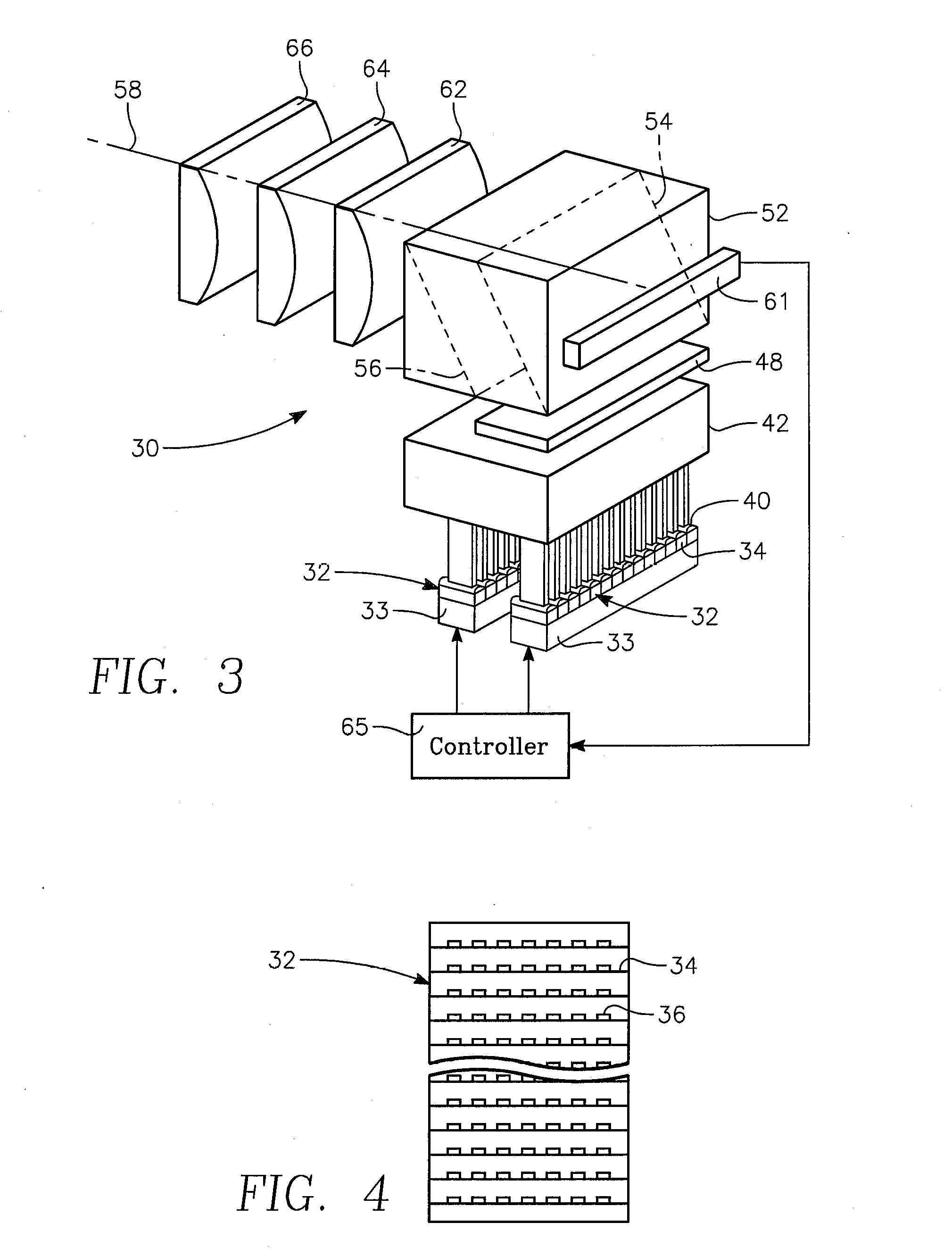
[0028]A DSA processing apparatus employs an imaging pyrometer, an imaging emissometer, and computer addressable laser diode array to compensate for absorption and reflectivity variations across the water. The addressable laser diode array energy is focused onto the semiconductor substrate surface for the purposes of DSA thermal processing. As the substrate is heated, the imaging emissometer and pyrometer measure the emmissivity and determine the temperature variation across the line beam image zone on semiconductor substrate surface produced by the addressable laser diode array through the focusing optics. The addressable laser diode array is intensity corrected by a programmed controller to compensate for variations detected by the emissometer and pyrometer. Essentially, a line of laser light is focused onto the semiconductor surface and individual zones or image elements along the laser line are temperature controlled by controlling the electrical current to like zone...


PUM

PropertyMeasurementUnit
temperaturesaaaaaaaaaa

Abstract

Apparatus for dynamic surface annealing of a semiconductor wafer includes a source of laser radiation emitting at a laser wavelength and comprising an array of lasers arranged in rows and columns, the optical power of each the laser being individual adjustable and optics for focusing the radiation from the array of lasers into a narrow line beam in a workpiece plane corresponding to a workpiece surface, whereby the optics images respective columns of the laser array onto respective sections of the narrow line beam. A pyrometer sensor is provided that is sensitive to a pyrometer wavelength. An optical element in an optical path of the optics is tuned to divert radiation emanating from the workpiece plane to the pyrometry sensor. As a result, the optics images each of the respective section of the narrow line beam onto a corresponding portion of the pyrometer sensor. The apparatus further includes a controller responsive to the pyrometry sensor and coupled to adjust individual optical outputs of respective columns of the laser array in accordance with outputs of corresponding portions of the pyrometry sensor.

Description

CROSS-REFERENCE TO RELATED APPLICATIONS[0001]This application claims the benefit of U.S. Provisional Application Ser. No. 60 / 817,131, filed Jun. 27, 2006.FIELD OF THE INVENTION[0002]The invention relates generally to thermal processing of semiconductor substrates. In particular, the invention relates to laser thermal processing of semiconductor substrates.BACKGROUND OF THE INVENTION[0003]Thermal processing is required in the fabrication of silicon and other semiconductor integrated circuits formed in silicon wafers or other substrates such as glass panels for displays. The required temperatures may range from relatively low temperatures of less than 250° C. to greater than 100° C. or 1300° C., for example, and may be used for a variety of processes such as dopant implant annealing, crystallization, oxidation, nitridation, silicidation, and chemical vapor deposition as well as others.[0004]For the very shallow circuit features required for advanced integrated circuits, it is greatly ...

Claims


Application Information

Patent Timeline
Patent Type & Authority Applications(United States)
IPC IPC(8): B23K26/42B23K26/04
CPCB23K26/03B23K26/032B23K26/034H01L21/67115B23K26/0738F27B17/0025B23K26/0665
Inventor THOMAS, TIMOTHY N.JENNINGS, DEANADAMS, BRUCE E.MAYUR, ABHILASH J.
Owner APPLIED MATERIALS INC
Why Eureka
Try Eureka