Wideband active balun circuit based on differential amplifier

a technology of differential amplifiers and balun circuits, applied in the field of wideband active balun circuits based on differential amplifiers, can solve the problems of difficult application of wideband active techniques, unbalance between two differential output signals, and unbalance between different output signals, so as to achieve the effect of increasing integration density advantages

Inactive Publication Date: 2008-05-29
ELECTRONICS & TELECOMM RES INST
View PDF3 Cites 22 Cited by
  • Summary
  • Abstract
  • Description
  • Claims
  • Application Information

AI Technical Summary

Benefits of technology

[0015]The present invention is directed to a wideband active balance-to-unbalance (balun) circuit, which can compensate for unbalance between two differential signals using CMOS devices that have increased integration density advantages.
[0016]Also, the present invention is directed to a wideband active balun circuit, which can compensate for unbalance between two differential signals by finely tuning errors in amplitude and phase between the two differential signals in a simple manner.
[0017]Furthermore, the present invention is directed to a wideband active balun circuit, which can prevent the occurrence of signal leakage and self-mixture due to interference between input and output nodes.
[0018]To achieve the above-described objects, the present invention provides a wideband active balance-to-unbalance (balun) circuit based on a differential amplifier, which converts a single-ended input signal into two phase-inverted differential signals having the same amplitude and outputs the two differential signals, wherein a dummy resistor and a dummy transistor are connected in series between a power supply voltage terminal and a drain terminal of a transistor used as a tail current source in order to compensate for unbalance between the two differential signals caused by a parasitic capacitance of the transistor used as the tail current source.

Problems solved by technology

In this case, the differential output signals become unbalanced due to a capacitive loading effect of a parasitic capacitor caused by the third NMOS transistor N23 functioning as a tail current source.
In particular, when an RF signal is applied to the active balun circuit 120, unbalance between the two differential output signals becomes more serious.
However, it is difficult to apply this technique to a wideband active balun circuit, and a chip area is increased due to a bulky inductor.

Method used


Image

  • Wideband active balun circuit based on differential amplifier
  • Wideband active balun circuit based on differential amplifier
  • Wideband active balun circuit based on differential amplifier

Examples


embodiment 1

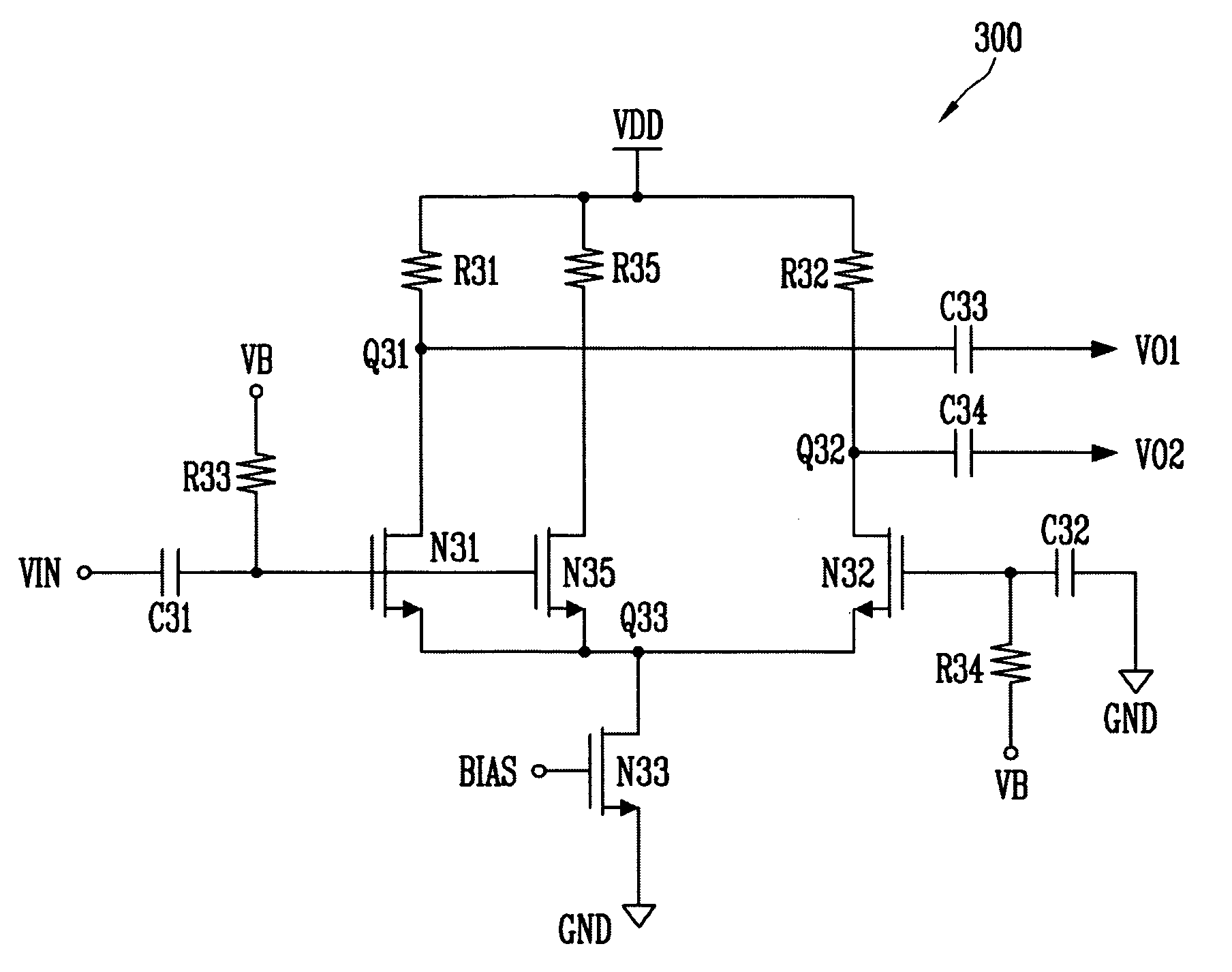
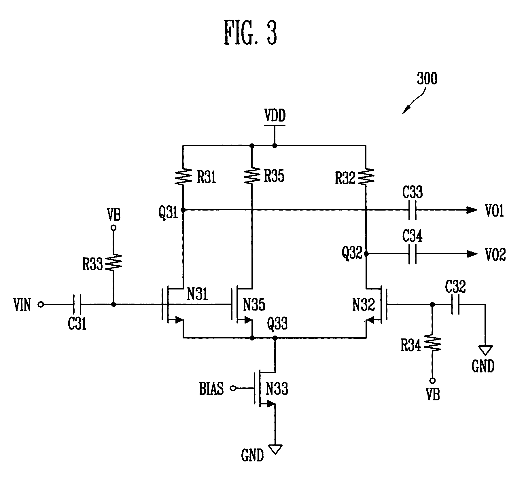
[0027]The construction of an active balance-to-unbalance (balun) circuit 300 will now be described with reference to FIG. 3.

[0028]Referring to FIG. 3, a first resistor R31 is connected between a power supply voltage terminal VDD and a first node Q31, and a second resistor R32 is connected between the power supply voltage terminal VDD and a second node Q32. Drain and source terminals of a first NMOS transistor N31 are connected between the first node Q31 and a third node Q33, and drain and source terminals of a second NMOS transistor N32 are connected between the second node Q32 and the third node Q33. A third NMOS transistor N33 having a gate terminal to which a predetermined bias voltage is applied by a bias terminal BIAS is connected between the third node Q33 and a ground terminal GND. A first capacitor C31 is connected between an input terminal VIN and a gate terminal of the first NMOS transistor N31, and a second capacitor C32 is connected between the ground terminal GND and a ...

embodiment 2

[0039]The construction of an active balun circuit 400 will now be described with reference to FIG. 4.

[0040]Referring to FIG. 4, a first resistor RI is connected between a power supply voltage terminal VDD and a first node Q41, and a second resistor R2 is connected between the power supply voltage terminal VDD and a second node Q42. Drain and source terminals of a first NMOS transistor N41 are connected between the first node Q41 and a third node Q43. Drain and source terminals of a second NMOS transistor N42 are connected between the second node Q42 and the third node Q43. A third NMOS transistor N43 having a gate terminal to which a predetermined bias voltage is applied by a bias terminal BIAS is connected between the third node Q43 and a ground terminal GND. A first capacitor C41 is connected between an input terminal VIN and a gate terminal of the first NMOS transistor N41, and a second capacitor C42 is connected between the ground terminal GND and a gate terminal of the second N...

embodiment 3

[0044]The construction of an active balun circuit 500 will now be described with reference to FIG. 5. The active balun circuit 500 can compensate for unbalance between two differential signals and prevent signal leakage and self-mixture caused by interference between input and output nodes.

[0045]Referring to FIG. 5, a first inductor L51 is connected between a power supply voltage terminal VDD and a first node Q51, and a second inductor L52 is connected between the power supply voltage terminal VDD and a second node Q52. A sixth NMOS transistor N56 and a first NMOS transistor N51, which are cascode transistors, are connected in series between the first node Q51 and a third node Q53. A seventh NMOS transistor N57 and a second NMOS transistor N52, which are cascode transistors, are connected in series between the second node Q52 and the third node Q53. A third NMOS transistor N53 having a gate terminal to which a predetermined bias voltage is applied by a bias terminal BIAS is connecte...


PUM


Abstract

Provided is a wideband active balun circuit based on a differential amplifier. The active balun circuit is configured to compensate for unbalance between two differential signals and can be applied to wideband systems, such as software defined radio (SDR) systems or ultra wideband (UWB) systems. Also, when signal unbalance is caused by changes in process conditions, such as temperature, errors in amplitude and phase between the two differential signals can be finely tuned by adjusting a voltage tuning terminal outside a chip, so that the active balun circuit can simply solve the unbalance between the two differential signals. Furthermore, input transistors that constitute a pair of differential amplifiers are provided in a cascode structure to prevent the occurrence of signal leakage and self-mixture.

Description

CROSS-REFERENCE TO RELATED APPLICATION[0001]This application claims priority to and the benefit of Korean Patent Application No. 2006-122524, filed Dec. 5, 2006, and No. 2007-54421, filed Jun. 4, 2007, the disclosure of which is incorporated herein by reference in its entirety.BACKGROUND[0002]1. Field of the Invention[0003]The present invention relates to a wideband active balance-to-unbalance (balun) circuit based on a differential amplifier and, more specifically, to a wideband balun circuit used for a radio-frequency (RF) transceiving system, which converts a single-ended RF input signal into two complementary differential output signals.[0004]This work was supported by the IT R&D program of Ministry of Information and Communication / Institute for Information Technology Advancement [2006-S-015-01, Development of Digital RF and ADC Chips for Multi-Mode SDR Terminal.][0005]2. Discussion of Related Art[0006]A wireless transceiving system wirelessly transmits and receives information ...

Claims


Application Information

Patent Timeline
Patent Type & Authority Applications(United States)
IPC IPC(8): H03F3/45H03H5/00
CPCH03F1/3211H03F3/195H03F3/45183H03F3/45188H03F3/45766H03F2200/06H03H11/32H03F2200/453H03F2203/45291H03F2203/45302H03F2203/45364H03F2203/45532H03F2200/09H03F3/265
Inventor PARK, SEONG SUCHOI, BYOUNG GUNMIN, BYUNG HUN
Owner ELECTRONICS & TELECOMM RES INST
Why Eureka
Try Eureka