Semiconductor device and method for fabricating the same

a technology of semiconductor integrated circuits and semiconductors, applied in the direction of semiconductor devices, electrical equipment, transistors, etc., can solve the disadvantageous reduction of the operation speed of the semiconductor integrated circuit, and achieve the effect of small gate line width and low interconnect resistan

Inactive Publication Date: 2008-06-05
PANASONIC CORP
View PDF0 Cites 22 Cited by
  • Summary
  • Abstract
  • Description
  • Claims
  • Application Information

AI Technical Summary

Benefits of technology

[0023]In the third method of the method for fabricating a semiconductor device according to the aspect of the invention, the step (a) includes a sub-step of forming a second active region surrounded with the isolation region in the semiconductor substrate, the step (d) includes a sub-step of forming a second p-type impurity diffusion region in a portion of the second active region disposed on a side of the second sidewall through ion implantation of a p-type impurity by using the second sidewall as a mask, a thickness of the second gate pattern silicon film is reduced on the second active region to be smaller than on the isolation region through etching using the resist mask pattern having a second opening pattern correspondingly to the second active region in the step (f), and the second fully silicided gate pattern including a second fully silicided gate line disposed on the isolation region and a second fully silicided gate electrode disposed on the second active region is formed in the step (g).
[0024]As described so far, according to the semiconductor device and the fabrication method for the same of this invention, with respect to a semiconductor device employing the fully silicided gate process with a small gate line width, a semiconductor device including a gate line with low interconnect resistance and a method for fabricating the same can be realized.

Problems solved by technology

In other words, the specific resistance of a fully silicided gate line portion extending, on an isolation region, from a fully silicided gate electrode of a pMISFET formed on an active region surrounded with the isolation region is so large that the operation speed of the semiconductor integrated circuit is disadvantageously lowered.

Method used


Image

  • Semiconductor device and method for fabricating the same
  • Semiconductor device and method for fabricating the same
  • Semiconductor device and method for fabricating the same

Examples


embodiment 1

[0037]A semiconductor device and a method for fabricating the same according to Embodiment 1 of the invention will now be described with reference to the accompanying drawings.

[0038]First, the structure of the semiconductor device of Embodiment 1 will be described with reference to FIGS. 1A through 1C.

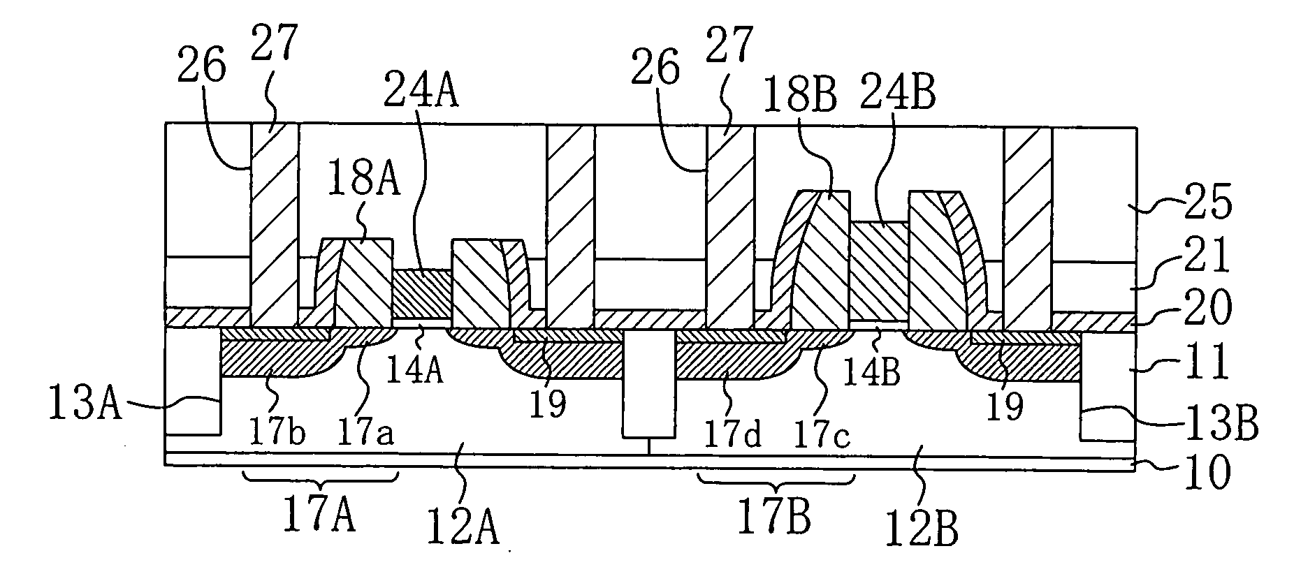
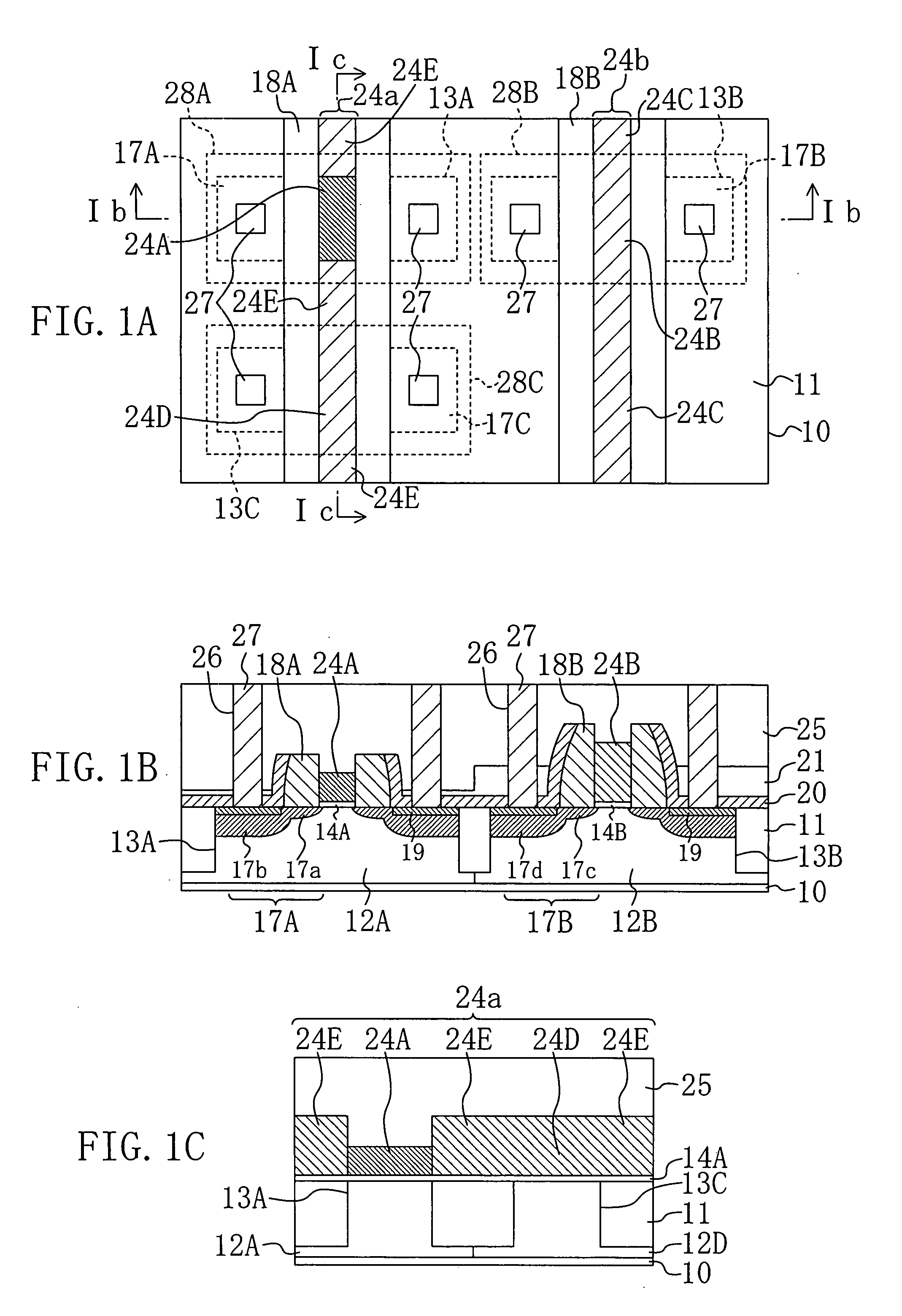
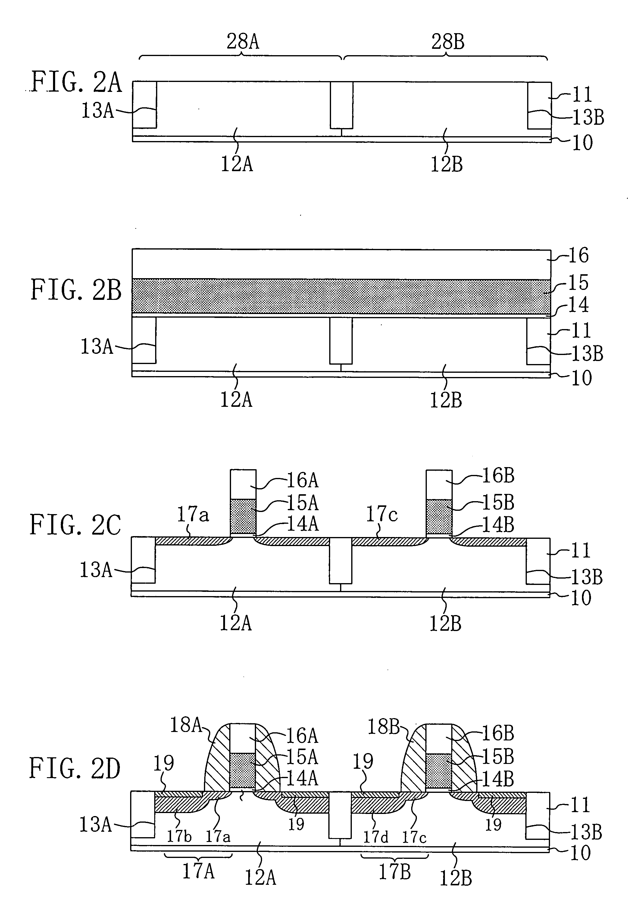
[0039]FIGS. 1A through 1C are diagrams for explaining the structure of the semiconductor device of Embodiment 1 of the invention, and specifically, FIG. 1A is a plan view thereof, FIG. 1B is a cross-sectional view thereof taken on line Ib-Ib of FIG. 1A and FIG. 1C is a cross-sectional view thereof taken on line Ic-Ic of FIG. 1A. It is noted that part of the structure correspondingly shown in FIGS. 1B and 1C is omitted in FIG. 1A for convenience of the explanation.

[0040]As shown in the plan view of FIG. 1A, a first active region 13A included in a p-type MIS transistor forming region 28A, a second active region 13B included in an n-type MIS transistor forming region 28B and a third activ...

embodiment 2

[0075]A semiconductor device and a method for fabricating the same according to Embodiment 2 of the invention will now be described with reference to the accompanying drawings. In Embodiment 2 of the invention, a semiconductor device and a fabrication method obtained by applying the semiconductor device and the method for fabricating the same according to Embodiment 1 of the invention for lowering the gate line resistance to an SRAM forming region will be described.

[0076]First, the structure of the semiconductor device of Embodiment 2 of the invention will be described with reference to FIGS. 7A and 7B.

[0077]FIGS. 7A and 7B are diagrams for explaining the structure of the semiconductor device of this embodiment, and specifically, FIG. 7A is a plan view thereof and FIG. 7B is a cross-sectional view thereof taken on line VIIb-VIIb of FIG. 7A. It is noted that part of the structure correspondingly shown in FIG. 7B is omitted in FIG. 7A for convenience of the explanation.

[0078]As shown ...


PUM


Abstract

A p-type MIS transistor includes a first gate insulating film formed on a first active region; and a first fully silicided gate pattern that is obtained by fully siliciding a silicon film, is formed to extend over the first active region with the first gate insulating film sandwiched therebetween, and includes a first fully silicided gate electrode provided on the first active region and a first fully silicided gate line provided on the isolation region. The first fully silicided gate pattern includes, along a gate width direction, a portion having a first thickness and including the first fully silicided gate electrode and portions each having a second thickness larger than the first thickness and respectively disposed on both sides of the portion having the first thickness.

Description

BACKGROUND OF THE INVENTION[0001]The present invention relates to a semiconductor device and a method for fabricating the same, and more particularly, it relates to a semiconductor device having a fully silicided gate electrode and a method for fabricating the same.[0002]In accordance with the recent technical development for higher integration, higher performance and higher speed of semiconductor integrated circuit devices, MISFETs have been more and more refined.[0003]In a method earnestly examined in accordance with the refinement of MISFETs for further reducing the thickness of a gate insulting film and suppressing increase of a gate leakage current derived from a tunnel current, a high dielectric constant material made of a metal oxide such as hafnium oxide (HfO2), hafnium silicate (HfSiO) or a hafnium silicate nitride (HfSiON) is used instead of SiO2 or SiON conventionally used as a gate insulating film material, so that a leakage current can be suppressed with keeping a large...

Claims


Application Information

Patent Timeline
Patent Type & Authority Applications(United States)
IPC IPC(8): H01L27/092H01L21/8238
CPCH01L21/28097H01L21/823835H01L21/82385H01L29/7833H01L21/823871H01L29/4975H01L29/66545H01L21/823864
Inventor SATO, YOSHIHIROOGAWA, HISASHI
Owner PANASONIC CORP
Why Eureka
Try Eureka