Multi-Finger Capacitor

a capacitor and finger technology, applied in capacitors, diodes, semiconductor/solid-state device details, etc., can solve the problem of achieve low ac coupling loss, reduce capacitance, and reduce the effect of ac coupling loss

Inactive Publication Date: 2008-06-05
INTEGRATED DEVICE TECH INC
View PDF7 Cites 19 Cited by
  • Summary
  • Abstract
  • Description
  • Claims
  • Application Information

AI Technical Summary

Benefits of technology

[0018]Accordingly, the present invention provides a multi-finger capacitor structure including a capacitor input node having a first set of conductive fingers, a capacitor output node having a second set of conductive fingers and interleaved with the first set of conductive fingers, and a conductive plate and / or pattern connected to the capacitor input node, and located between a substrate and the first and second sets of interleaved conductive fingers. The conductive plate / pattern renders the parasitic capacitance of the capacitor output node negligible, thereby resulting in a low AC coupling loss. The low AC coupling loss enables the multi-finger capacitor structure of the present invention to have a lower capacitance than a conventional multi-finger capacitor, for the same application. As a result, the multi-finger capacitor structure of the present invention can have a significantly smaller layout area, and have significantly lower driver power requirements, than a conventional multi-finger capacitor structure.

Problems solved by technology

The conductive plate / pattern renders the parasitic capacitance of the capacitor output node negligible, thereby resulting in a low AC coupling loss.

Method used


Image

  • Multi-Finger Capacitor
  • Multi-Finger Capacitor
  • Multi-Finger Capacitor

Examples


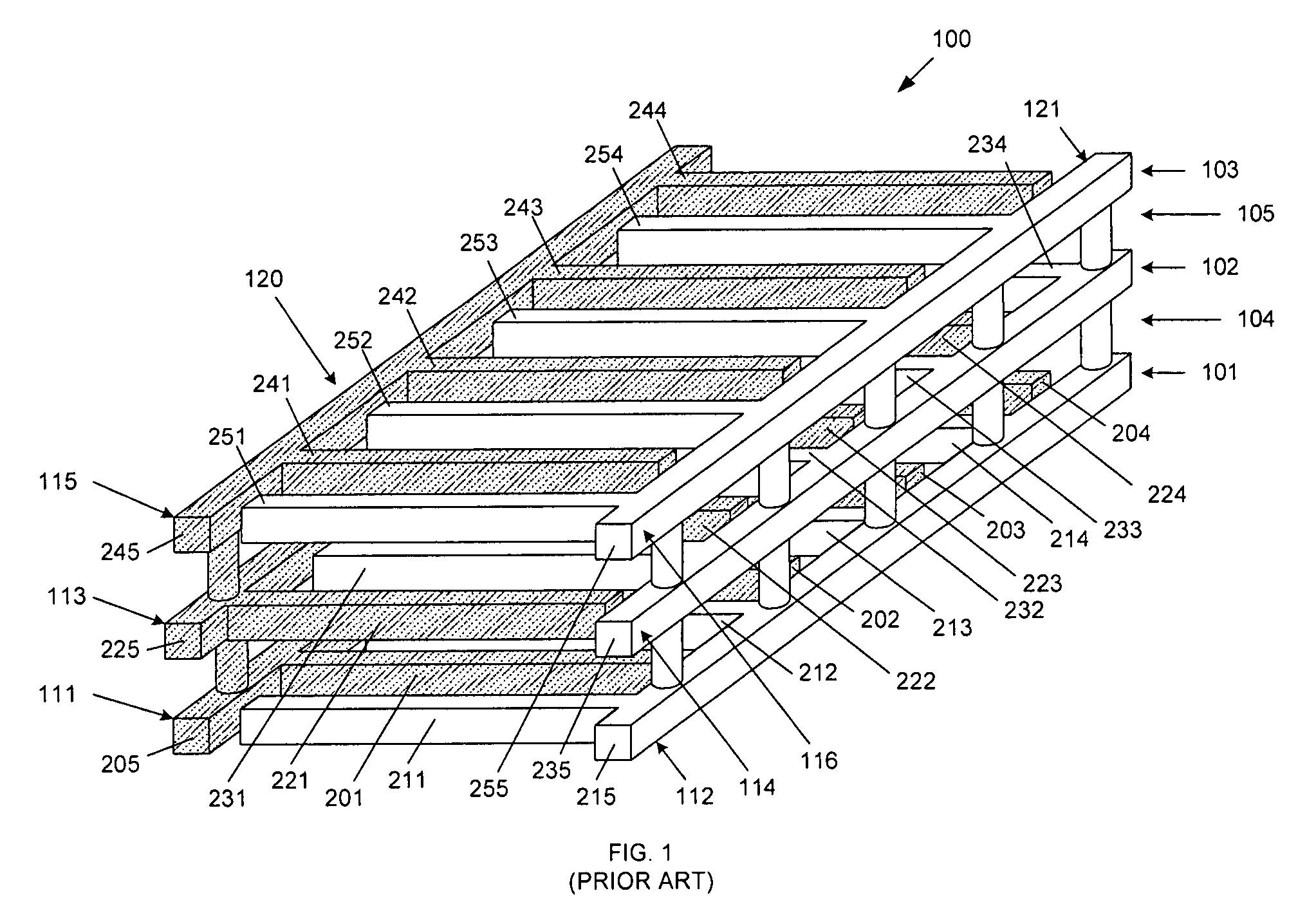
Embodiment Construction

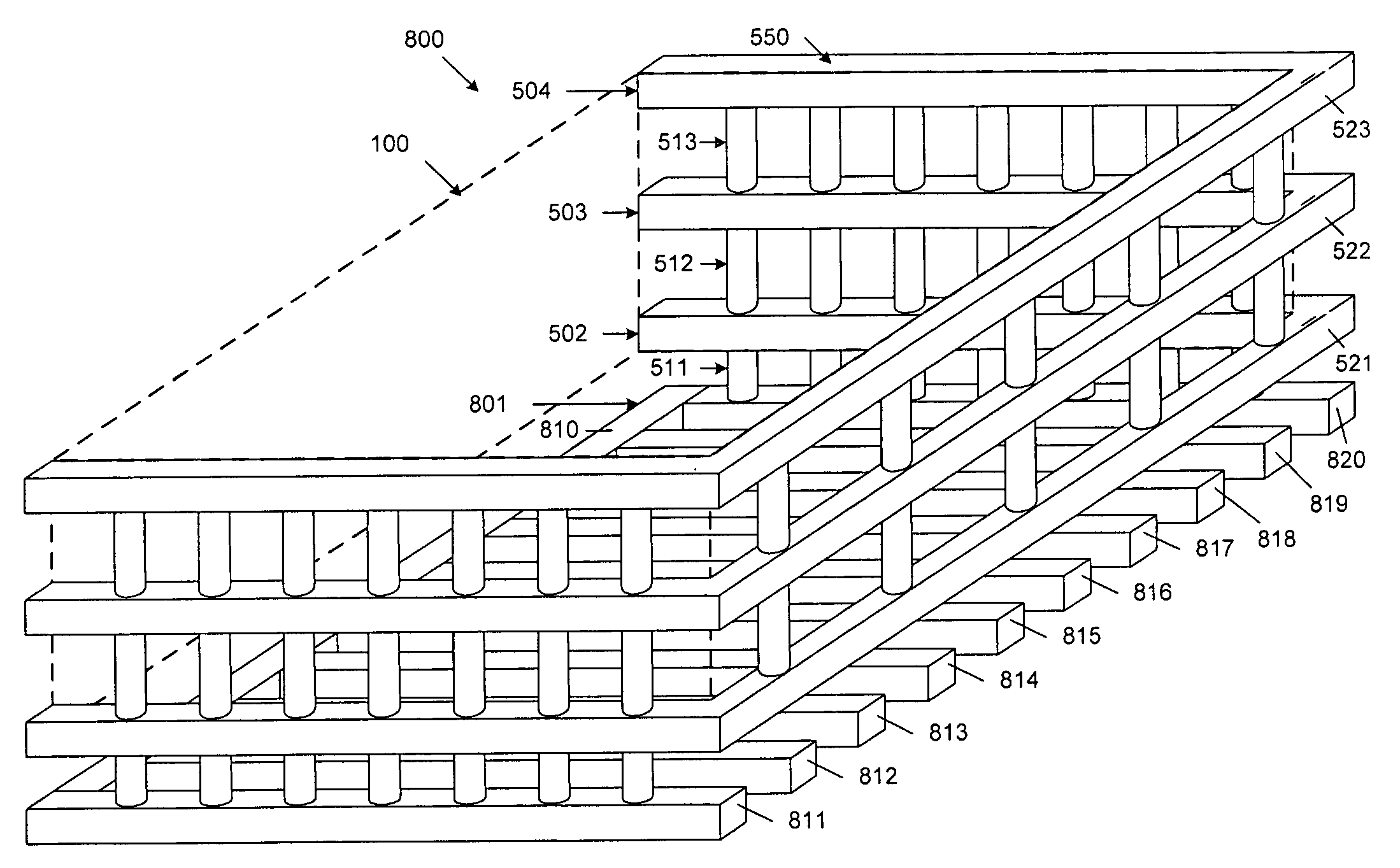
[0029]FIG. 5 is an isometric view of a multi-finger capacitor structure 500 in accordance with one embodiment of the present invention. Capacitor structure 500 includes the multi-finger capacitor 100 of FIG. 1 (which is illustrated as a dashed box in FIG. 5 for purposes of clarity), and a metal cage structure 550, which is electrically connected to the input node 120 of multi-finger capacitor 100. The manner in which the multi-finger capacitor 100 is coupled to the metal cage structure 550 is described in more detail below.

[0030]In the described embodiments, metal cage structure 550 includes four metal layers 501-504 and three via layers 511-513, which are formed over an underlying substrate (not shown in FIG. 5). In the embodiment illustrated by FIG. 5, the first metal layer 501 includes a metal plate 520, which is isolated from the underlying substrate by a dielectric material (not shown). The first via layer 511 provides one or more electrical connections between metal plate 520 ...


PUM


Abstract

A multi-finger capacitor structure includes a capacitor input node having a first set of conductive fingers, a capacitor output node having a second set of conductive fingers interleaved with the first set of conductive fingers, and a conductive plate and/or pattern connected to the capacitor input node, and located between a substrate and the first and second sets of interleaved conductive fingers. The conductive plate/pattern renders the parasitic capacitance of the capacitor output node negligible, thereby imparting desirable operating characteristics to the capacitor structure. The capacitor input node may also include Faraday electric walls that laterally surround the capacitor output node, thereby limiting electrical energy leakage.

Description

RELATED APPLICATION [0001]The present application is related to, and claims priority of, U.S. Provisional Patent Application Ser. No. 60 / 868,668 filed by Han Bi on Dec. 5, 2006.FIELD OF THE INVENTION [0002]The present invention relates to multi-finger capacitors. More specifically, the present invention relates to multi-finger capacitors used for alternating current (AC) signal coupling.RELATED ART [0003]Analog integrated circuits, such as SERDES I / O circuits, often require high quality capacitors for AC signal coupling. For example, a high-quality capacitor may be used to implement capacitive AC coupling in the last stage of a multi-stage current mode logic clock buffer, in order to remove the accumulated duty cycle error.[0004]FIG. 1 is an isometric diagram of a conventional multi-finger capacitor 100 used for the above-described purpose. Capacitor 100 is formed by multiple metal layers 101-103, which are joined by multiple via layers 104-105 of a semiconductor process. The first ...

Claims


Application Information

Patent Timeline
Patent Type & Authority Applications(United States)
IPC IPC(8): H01L29/86
CPCH01L23/5223H01L28/60H01L27/0805H01L2924/0002H01L2924/00
Inventor BI, HAN
Owner INTEGRATED DEVICE TECH INC
Why Eureka
Try Eureka