Plasma display panel and field emission display

a display panel and field emission technology, applied in the field of plasma display panels, can solve the problems of insufficient anti-reflection function of cone-shaped or pyramid-shaped anti-reflection structures, and the difficulty of detecting incident light rays from external sources, etc., and achieve the effects of high performance, efficient dispersion, and high definition

Inactive Publication Date: 2008-06-05
SEMICON ENERGY LAB CO LTD
View PDF38 Cites 26 Cited by
  • Summary
  • Abstract
  • Description
  • Claims
  • Application Information

AI Technical Summary

Benefits of technology

[0014]The PDP and the FED of the present invention are each provided with an anti-reflection layer having a plurality of hexagonal pyramid-shaped projections arranged without any space remaining on a surface. Since a surface of a side of a hexagonal pyramid-shaped projection is not a plane surface (a surface parallel to a display screen), incident light from external source does not reflect to a viewer side but reflects on another adjacent hexagonal pyramid-shaped projection, or travels between the hexagonal pyramid-shaped projections. In addition, the hexagonal pyramid-shaped with a hexagonal base has a form which can be provided in a close-packed manner without any space remaining and among such forms this form has the largest number of surfaces of side thereof, light can be efficiently dispersed in a plurality of directions, so that it is an optimum form which can function well in an anti-reflection sense. Incident light from external source is partly transmitted thro

Problems solved by technology

Further, for mutual cancellation of incident light from an external source, it is necessary to precisely control optical characteristics, thicknesses, and the like of materials of films that are stacked, and it has been difficult to pe

Method used


Image

  • Plasma display panel and field emission display
  • Plasma display panel and field emission display
  • Plasma display panel and field emission display

Examples


embodiment mode 1

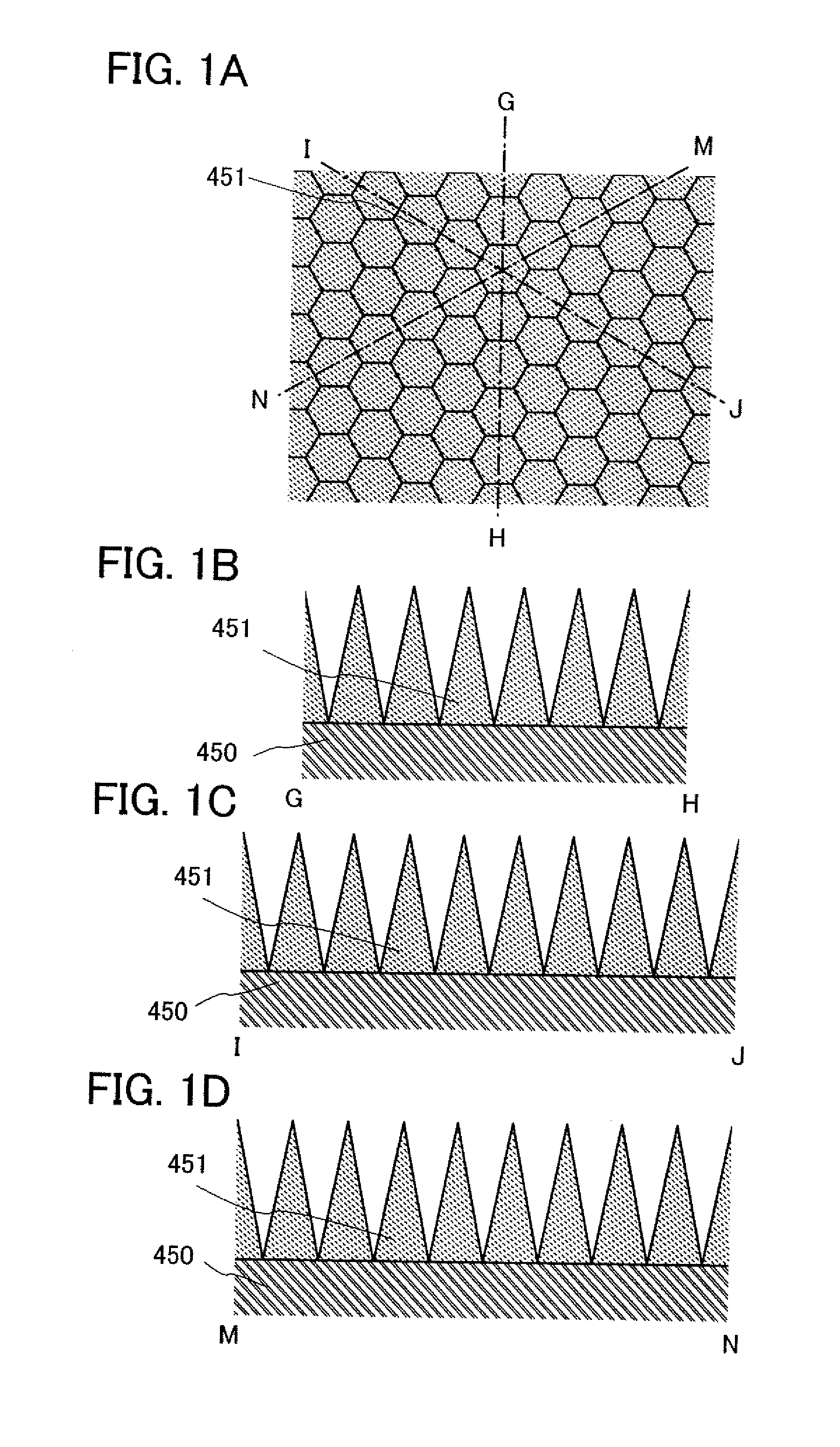
[0047]This embodiment mode will describe an anti-reflection layer which is provided to a PDP and an FED in the present invention. Specifically, an example of an anti-reflection layer having an anti-reflection function capable of further reducing reflection of incident light on a surface of a PDP or an FED from an external source, thereby providing the PDP or FED with excellent visibility, will be described.

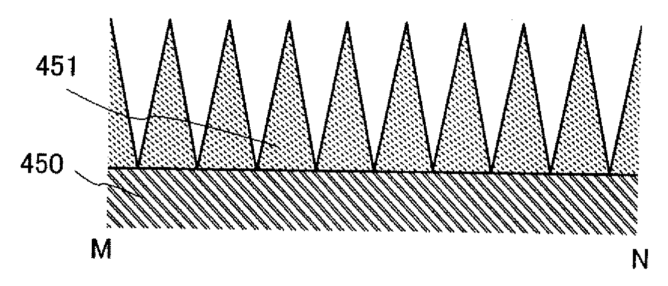
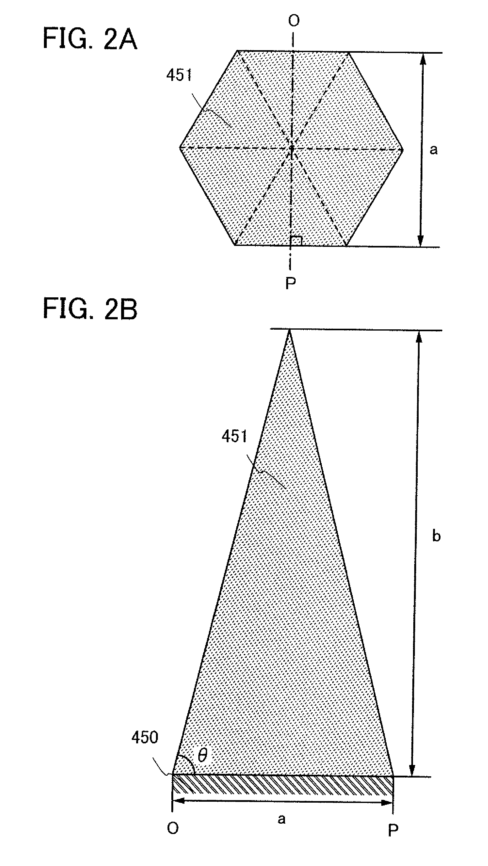
[0048]FIGS. 1A to 1D show a top view and cross-sectional views of an anti-reflection layer of the present invention. In FIGS. 1A to 1D, a plurality of hexagonal pyramid-shaped projections 451 are provided on a substrate 450 which serves as a display screen. The anti-reflection layer is formed from the plurality of hexagonal pyramid-shaped projections 451. FIG. 1A is a top view of the PDP or the FED of this embodiment mode, FIG. 1B is a cross-sectional view taken along a line G-H in FIG. 1A, FIG. 1C is a cross-sectional view taken along a line I-J in FIG. 1A, and FIG. 1D is a cross...

embodiment mode 2

[0081]In this embodiment mode, a PDP aimed at having an anti-reflection function capable of further reducing reflection of incident light from an external source and providing excellent visibility will be described. That is, details of a structure of a PDP including a pair of substrates, a pair of electrodes interposed between the pair of substrates, a phosphor layer interposed between the pair of electrodes, and an anti-refection layer provided on an outer side of one of the pair of substrates will be described.

[0082]In this embodiment mode, a surface discharge PDP of alternating current discharge type (an AC type) is shown. As shown in FIG. 9, in a PDP, a front substrate 110 and a rear substrate 120 face each other, and the periphery of the front substrate 110 and the rear substrate 120 is sealed with a sealing material (not shown). In addition, a gap between the front substrate 110, the rear substrate 120, and the sealant is filled with a discharge gas.

[0083]Discharge cells of a ...

embodiment mode 3

[0130]In this embodiment mode, an FED aimed at having an anti-reflection function which can reduce reflection of incident light from an external source and providing excellent visibility will be described. That is, details of a structure of FED including a pair of substrates, a field emission element provided for one of the pair of substrates, an electrode provided for the other pair of substrates, a phosphor layer which is in contact with the electrode, and an anti-reflection layer provided on an outer side of the other substrate will be described.

[0131]A FED is a display in which a phosphor is exited by an electron beam to emit light. A FED can be classified into a diode FED, a triode FED, and a tetrode FED according to the structure of electrodes.

[0132]The diode FED has a structure in which a rectangular cathode electrode is formed on a surface of a first electrode, a rectangular anode electrode is formed on a surface of a second substrate, and the cathode electrode and the anode...


PUM


Abstract

To provide a plasma display panel and a field emission display having an anti-reflection function which can further reduce reflection of incident light from an external source. By providing an anti-reflection layer which geometrically includes a plurality of adjacent hexagonal pyramid-shaped projections, reflection of light is prevented. The reflective index changes from a surface side of display screen to an out side (an atmosphere side) due to a physical shape of a hexagonal pyramid. The plurality of hexagonal pyramid-shaped projections can be provided densely without any space remaining, and six surfaces of side of the hexagonal pyramid-shaped projection are each provided at different angles to a base surface. Therefore, light ray can be effectively scattered in many directions.

Description

TECHNICAL FIELD[0001]The present invention relates to a plasma display panel having an anti-reflection function and a field emission display having an anti-reflection function.BACKGROUND ART[0002]In various displays (plasma display panels (hereinafter referred to as PDPs), field emission display (hereinafter referred to as FEDs), and the like), there may be cases where it becomes difficult to see a display screen due to reflection of its surroundings by surface reflection of incident light from an external source; accordingly, visibility is decreased. This is a considerable problem particularly in enlargement of display devices and outdoor use thereof.[0003]For preventing such reflection of incident light from an external source, a method for providing display screens of PDPs and FEDs with an anti-reflection film has been employed. For example, there is a method for providing an anti-reflection film that has a multilayer structure of stacked layers having different refractive indexe...

Claims


Application Information

Patent Timeline
IPC IPC(8): H01J1/62H01J17/49B82B3/00B82Y40/00B82Y99/00G09F9/00H01J11/22H01J11/24H01J11/34H01J11/36H01J11/38H01J11/40H01J11/42H01J11/44H01J11/50H01J29/89H01J31/12
CPCH01J11/12H01J11/44H01J29/28H01J2329/892H01J31/127H01J2211/442H01J2211/444H01J29/86
Inventor EGI, YUJINISHIDA, JIRONISHI, TAKESHIYAMAZAKI, SHUNPEI
Owner SEMICON ENERGY LAB CO LTD
Why Eureka
Try Eureka