
Semiconductor storage device

a storage device and semiconductor technology, applied in semiconductor devices, digital storage, instruments, etc., can solve the problems of degrading the electrical characteristics of the input/output control circuit b>13/b>, the pitch of the pad cannot be reduced, and the excess region cannot be eliminated, so as to reduce the lateral width of the pad forming region, reduce the number of pad pitches, and eliminate the excess region

Active Publication Date: 2008-06-05
LAPIS SEMICON CO LTD
View PDF3 Cites 0 Cited by
  • Summary
  • Abstract
  • Description
  • Claims
  • Application Information

AI Technical Summary

Benefits of technology

The present invention provides a semiconductor storage device with a memory array section and a plurality of first and second pads arranged on a substrate. The first output transistors are formed near the first pads and the second output transistors are formed near the second pads. The second pads are arranged on the inner side of the first pads and the first transistors, second transistors, third transistors, and fourth transistors are arranged near each pad. This eliminates an excess region and reduces the chip size of the semiconductor storage device. The method of reducing an excess region on a semiconductor storage device includes arranging a memory array section and a plurality of first pads near one side of the substrate. The plurality of second pads are arranged on the inner side of the first pads and the first output transistors are formed near the first pads. The second output transistors are formed near the second pads. The semiconductor storage system includes a means for reducing a lateral width of the pad forming region for receiving a plurality of data pads and a means for eliminating an excess region between the data pads. The technical effects of this invention include reducing the chip size of the semiconductor storage device and improving the efficiency of the memory array.

Problems solved by technology

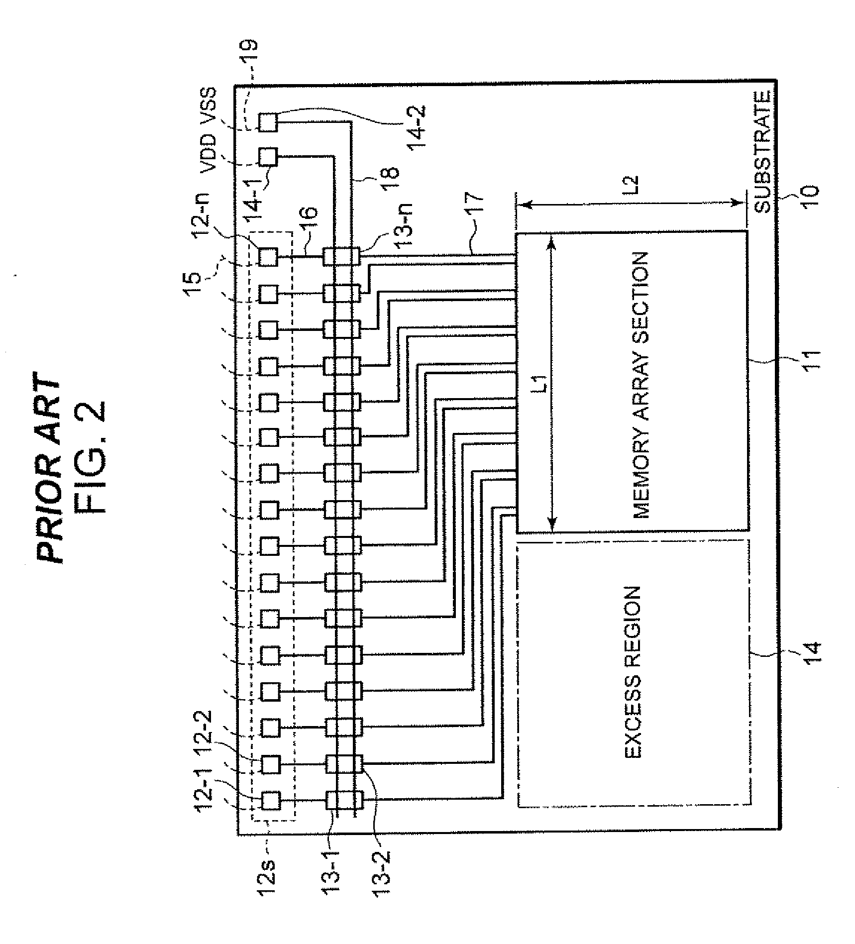
However, the semiconductor storage device shown in FIG. 2 has the following disadvantage.
However, in regard to the data pads 12 to be wire-bonded, a pad pitch which indicates a distance between the data pads 12-1 and 12-2 cannot be reduced because of a mechanical limitation of a wire bonding device.
Additionally, when the distance between the data pads 12 and the input / output control circuits 13 is small, there is a problem that electrical characteristics of the input / output control circuits 13 are degraded due to noise from the data pads 12.

Method used


Image

  • Semiconductor storage device
  • Semiconductor storage device
  • Semiconductor storage device

Examples


embodiment 1

Effects of Embodiment 1

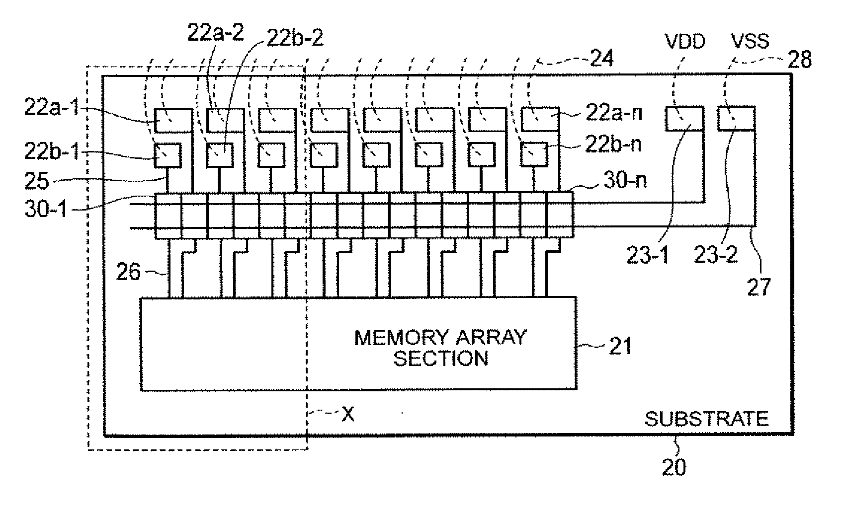
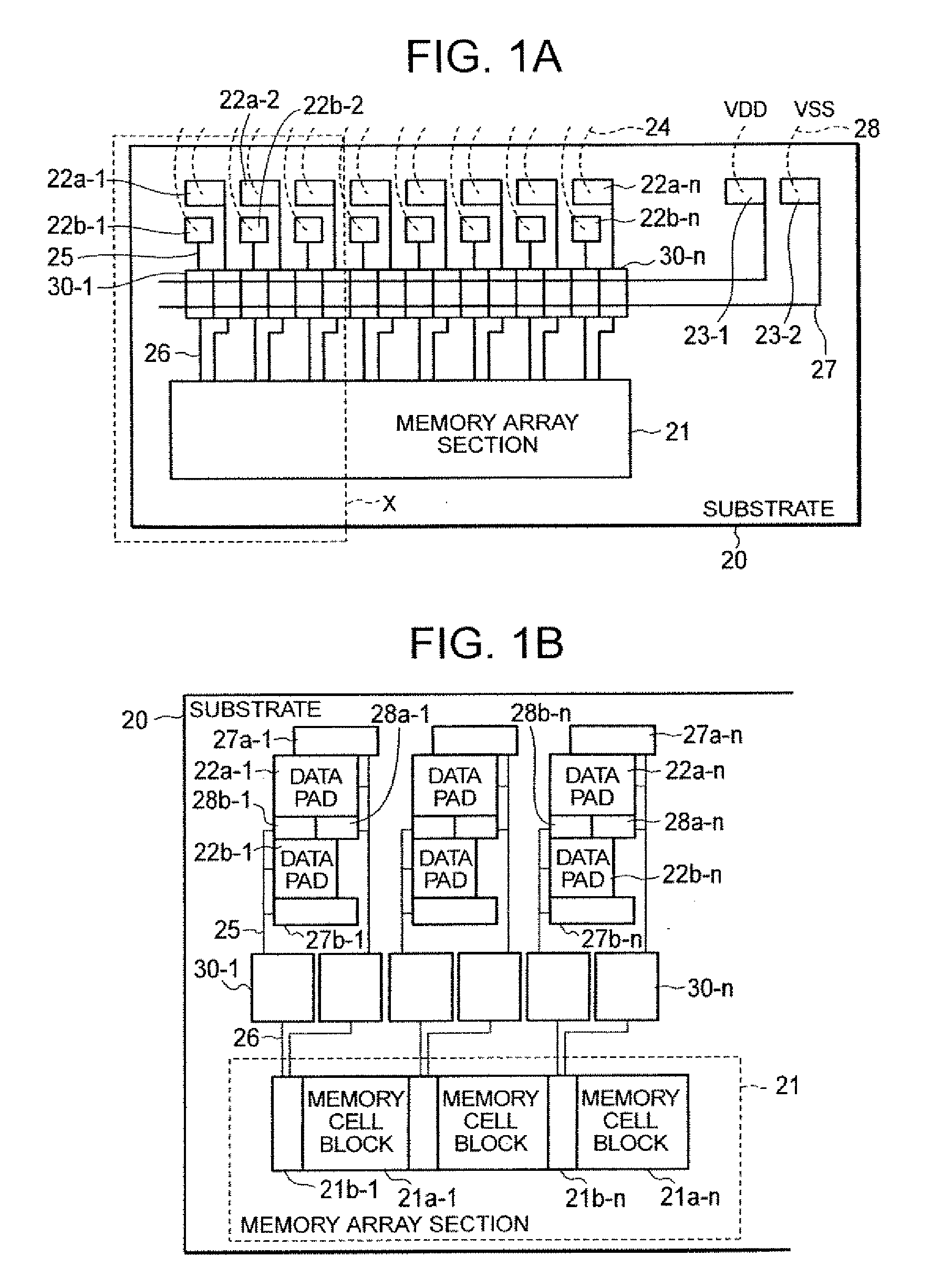
[0039]According to the semiconductor storage device of Embodiment 1, since the plurality of data pads 31b which input / output data are arranged on the inner side of the plurality of data pads 31a in parallel with the plurality of data pads 31 and the PMOS 36a, the PMOS 36b, the NMOS 37a, and the NMOS 37b are arranged near the respective data pads 31a and 31b, the following effects (A) to (D), as described herein, can be obtained.

[0040](A) A lateral width of a pad forming region where the data pads 27a or 27b are formed can be reduced. Therefore, an excess region is eliminated, thereby reducing a chip size.

[0041](B) Since the NMOSs 28a and 28b are arranged between the plurality of data pads 22a and the plurality of data pads 22b, an excess region between the plurality of data pads 22a and the plurality of data pads 22b is eliminated, and a pad pitch of the plurality of data pads 22a and the input output circuits 30 can be reduced, thereby decreasing the chip siz...

embodiment 2

Effects of Embodiment 2

[0050]According to the semiconductor storage device according to Embodiment 2, since the plurality of power supply pads 41a and 42b are arranged between the plurality of data pads 31a and 31b and the ESDs 42a, 42b, 43a, and 43b are provided, the following effects can be obtained in addition to the effects of Embodiment 1.

[0051]Since the power supply wire 28, the data wire 24, the data wire 24, and the power supply wire 28 are drawn out in the same direction in the mentioned order, a mutual inductance between pieces of data can be reduced, and an effect of decreasing slowdown in output due to an inductance at the time of reverse data output can be obtained.

[0052]Further, providing the ESDs 42a, 42b, 43a, and 43b enables protecting the semiconductor device from static electricity.

[0053](Modification)

[0054]The present invention is not restricted to Embodiments 1 and 2, and various use conformations and modifications can be carried out. As the use conformations or...


PUM


Abstract

An excess region on a chip plane is eliminated to reduce a chip size. A plurality of data pads, which input / output data, are arranged near one side of an outer periphery of a substrate in parallel with the aforementioned one side, and a plurality of data pads, which input / output data, are arranged on an inner side of the plurality of data pads in parallel with the plurality of data pads. NMOSs, which output data, are arranged between the data pads, and PMOSs, which output data, are arranged at positions where they face the NMOSs near the data pads.

Description

CROSS REFERENCE TO RELATED DOCUMENTS[0001]This application claims priority under 35 U.S.C § 119 to Japanese Patent Application Serial No. 2006328369 filed Dec. 5, 2006, the entire disclosure of which is hereby incorporated by reference herein.BACKGROUND OF THE INVENTION[0002]1. Field of the Invention[0003]The present invention relates to a semiconductor storage device, e.g., a dynamic random access memory (which will be referred to as a “DRAM” hereinafter) accommodated in a system in package (which will be referred to as an “SiP” hereinafter). For example, the present invention relates to a layout structure of data input / output pads associated with a plurality of bits, power supply pads, input / output control circuits which control over, e.g., writing / reading data, and others.[0004]2. Description of the Related Art[0005]Prior art examples including a layout of a semiconductor storage devices having data pads associated with a plurality of bits are shown in Japanese Patent Application...

Claims


Application Information

Patent Timeline
Patent Type & Authority Applications(United States)
IPC IPC(8): G11C5/06
CPCG11C5/025G11C11/412H01L24/06H01L2924/13091H01L2924/00H01L2224/05553H01L2224/05554H01L2224/0603H01L2924/14G11C11/40
Inventor NASU, NOBUTAKA
Owner LAPIS SEMICON CO LTD
Learn More