Method for doping impurities

a technology of impurities and solid phase diffusion, which is applied in the direction of semiconductor/solid-state device manufacturing, basic electric elements, electric devices, etc., can solve problems such as matrix damag

Active Publication Date: 2008-06-05
GENERAL ELECTRIC CO
View PDF12 Cites 40 Cited by
  • Summary
  • Abstract
  • Description
  • Claims
  • Application Information

AI Technical Summary

Benefits of technology

[0005]One embodiment of the present invention is a method for doping impurities into a device layer. The method includes providing a carbonized dopant layer over a device layer, wherein the carbonized dopant layer comprises one or more dopant impurities, and heat treating the carbonized dopant layer to thermally diffuse the dopant impurities into the device layer.
[0006]Another embodiment of the present invention is a method for doping impurities into a device layer with the method including disposing a carbon-based dopant material, wherein the carbon-based dopant material comprises one or more dopant impurities, carbonizing the carbon-based material to form a carbonized dopant layer, and heat treating the carbonized dopant layer to thermally diffuse the dopant impurities into t...

Problems solved by technology

Although ion implantation can be selectively performed, it often leaves a damaged matri...

Method used


Image

  • Method for doping impurities
  • Method for doping impurities
  • Method for doping impurities

Examples


example 1

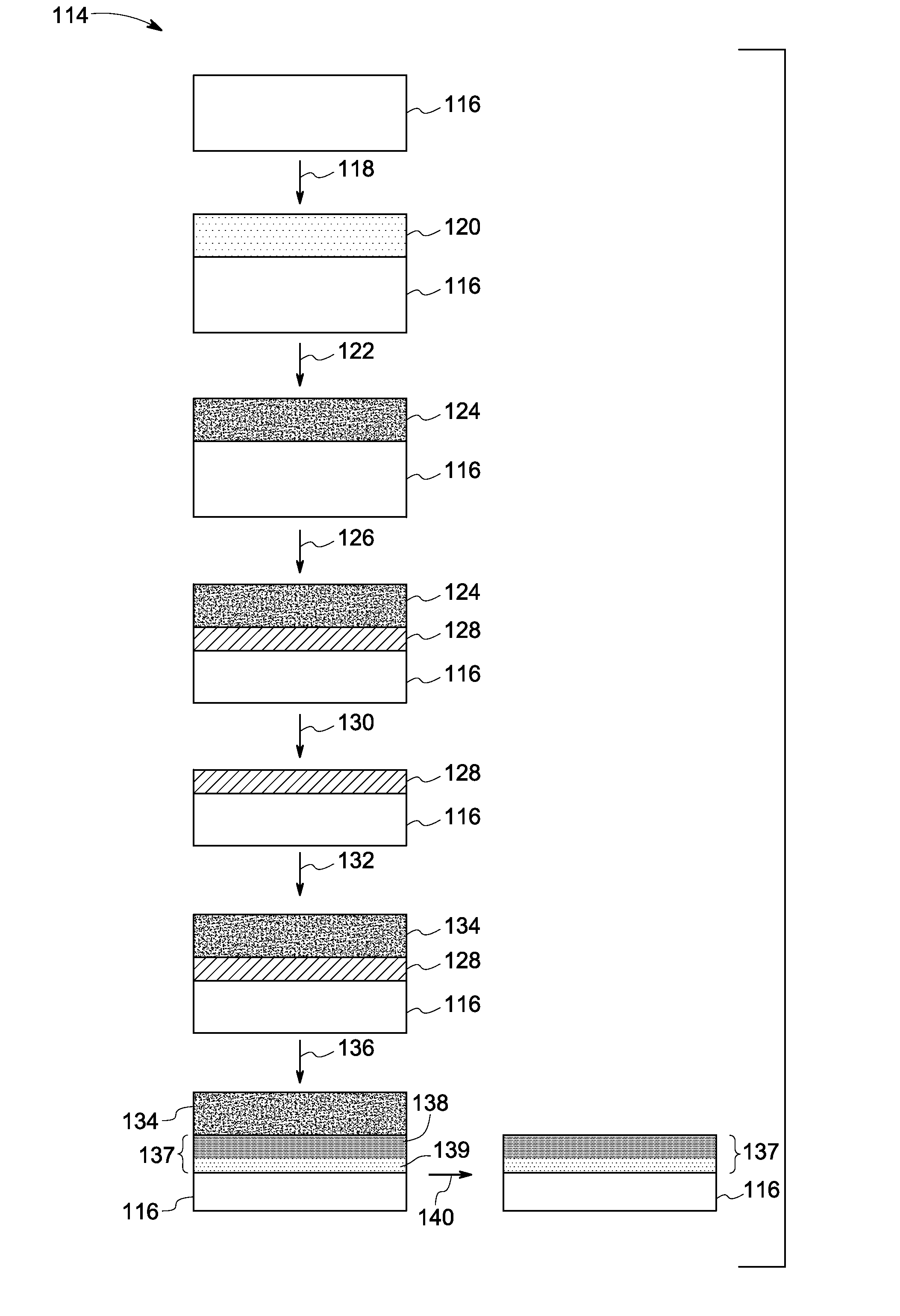
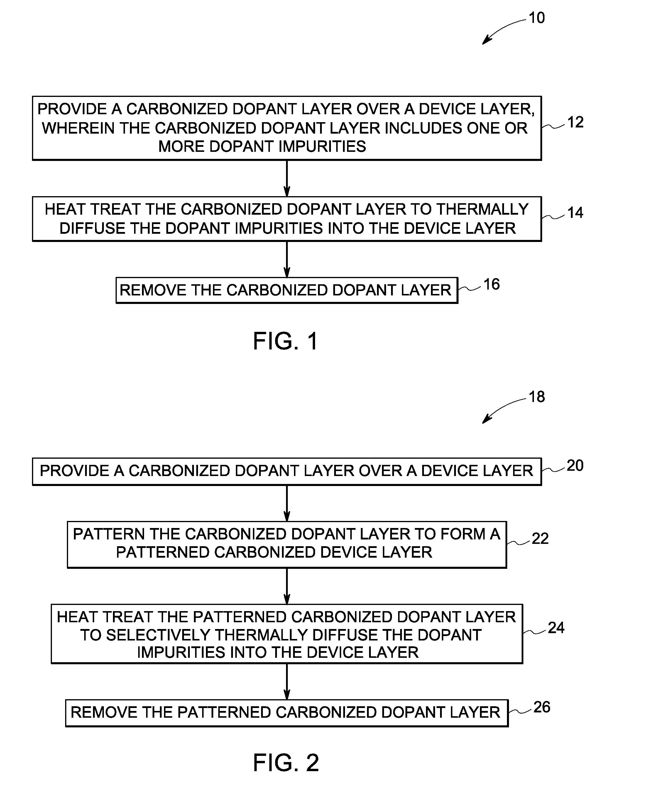
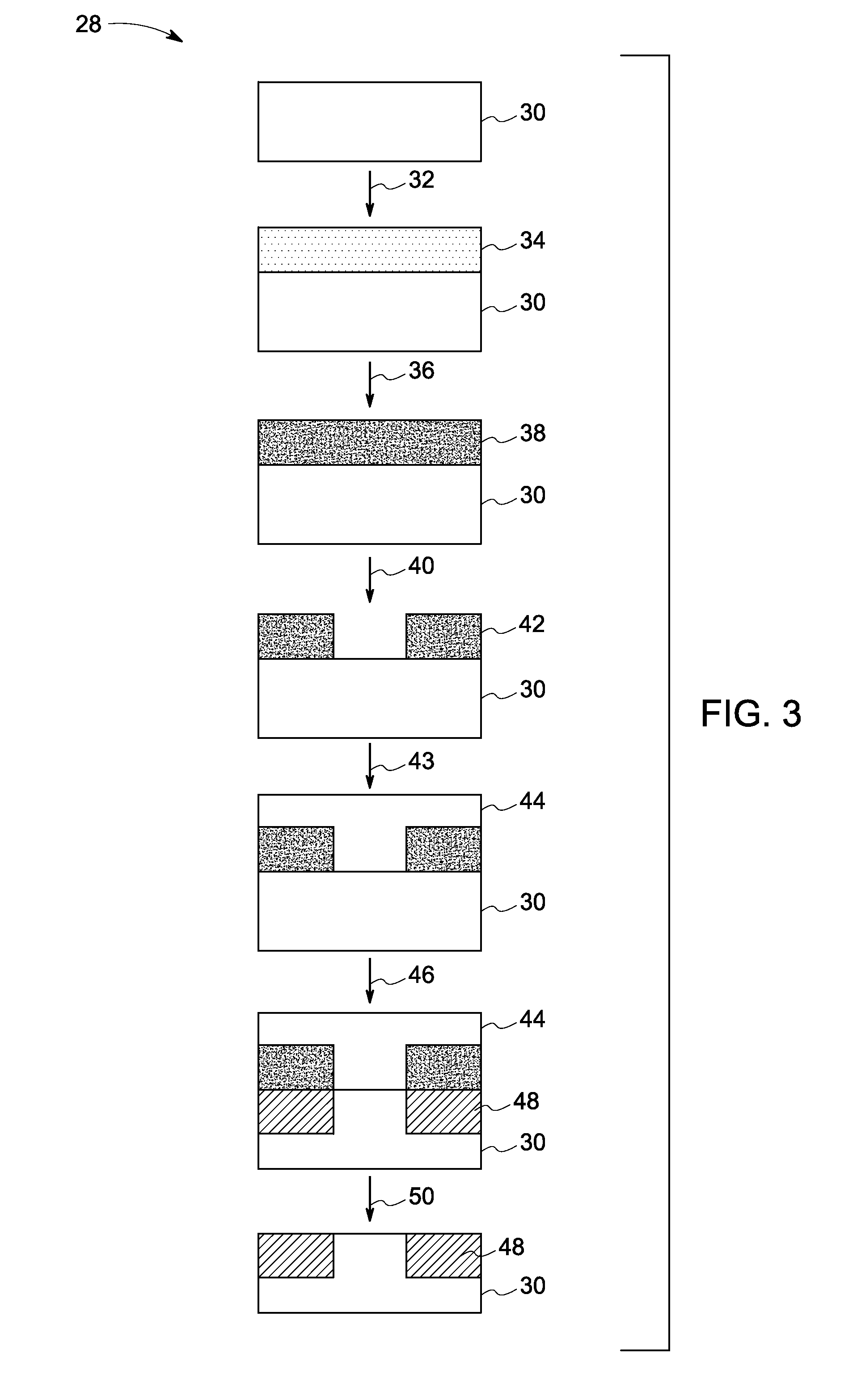
[0041]In one example a carbon-based dopant material is prepared by mixing a polymer photoresist (Shipley's AZ1518 or AZ1512) and a significant source of dopant (boron), tri-methyl-borate. The mixture is then evenly coated on a silicon carbide wafer by applying the mixture and spinning the silicon carbide wafer. The silicon carbide wafer coated with a carbon-based dopant layer is then annealed in a non-oxidizing ambient to drive off hydrogen and oxygen, leaving a carbonized dopant layer heavily laden with the boron impurity. The doped layer is patterned using photolithography, or is selectively etched away to accomplish selective area doping. To protect the exposed silicon carbide surface during the high temperature annealing step, the exposed area is then coated with an undoped photoresist. The silicon carbide wafer coated with the doped and patterned carbonized dopant layer is then annealed at a temperature of about, 1800° C. to about 2100° C., during which the impurities diffuse i...

example 2

[0042]In another example, a carbon-based dopant material is prepared by mixing a polymer photoresist (Shipley's AZ1518 or AZ1512) and a significant source of dopant (magnesium), Mg(OH)2. The mixture is then evenly coated on a gallium nitride wafer by applying the mixture and spinning the gallium nitride wafer. The gallium nitride wafer with the carbonized dopant layer is then annealed at temperature of about 1000° C. to about 1500° C., during which the impurities diffuse into the gallium nitride wafer.

[0043]Embodiments of the present invention are expected to provide selective doping and high quality surface with little damage to the lattice.


PUM


Abstract

A method for doping impurities into a device layer is provided. The method includes providing a carbonized dopant layer over a device layer, wherein the carbonized dopant layer comprises one or more dopant impurities, and heat treating the carbonized dopant layer to thermally diffuse the dopant impurities into the device layer.

Description

BACKGROUND[0001]The invention relates generally to a method for doping impurities into semiconductor device layers and more particularly, the invention relates to a solid phase diffusion method for doping impurities into semiconductor device layers.[0002]Currently, doped areas in wafers are created in one of a few ways. In one method, a semiconductor layer is grown with the dopant impurity in the gas stream during epitaxial growth of the semiconductor layer. The wafer can then be patterned and etched leaving doped regions. Epitaxy is typically conformal and non-selective.[0003]In another method, a pattern is made on a wafer or on top of an epitaxially grown layer. Impurities are then ion implanted by controlling the dose and power. Although ion implantation can be selectively performed, it often leaves a damaged matrix and requires a subsequent annealing process to embed the dopant impurity within the matrix.[0004]A method for doping impurities without the drawbacks of the current t...

Claims


Application Information

Patent Timeline
IPC IPC(8): H01L21/425
CPCH01L21/2258H01L21/0455
Inventor DUNNE, GREG THOMASTUCKER, JESSE BERKLEYSOLOVIEV, STANISLAV IVANOVICHSTUM, ZACHARY MATTHEW
Owner GENERAL ELECTRIC CO
Why Eureka
Try Eureka