

Film formation apparatus for semiconductor process and method for using the same
a technology of film formation apparatus and semiconductor device, which is applied in the direction of coating, chemical vapor deposition coating, electric discharge tube, etc., can solve the problems of deteriorating productivity, reducing the yield of semiconductor device to be manufactured, deteriorating some components of processing apparatus, and peeling of some by-product films, etc., to achieve the effect of not lowering productivity
- Summary
- Abstract
- Description
- Claims
- Application Information
AI Technical Summary
Benefits of technology
Problems solved by technology
Method used
Image

Examples
Embodiment Construction
[0024]Embodiments of the present invention will now be described with reference to the accompanying drawings. In the following description, the constituent elements having substantially the same function and arrangement are denoted by the same reference numerals, and a repetitive description will be made only when necessary.
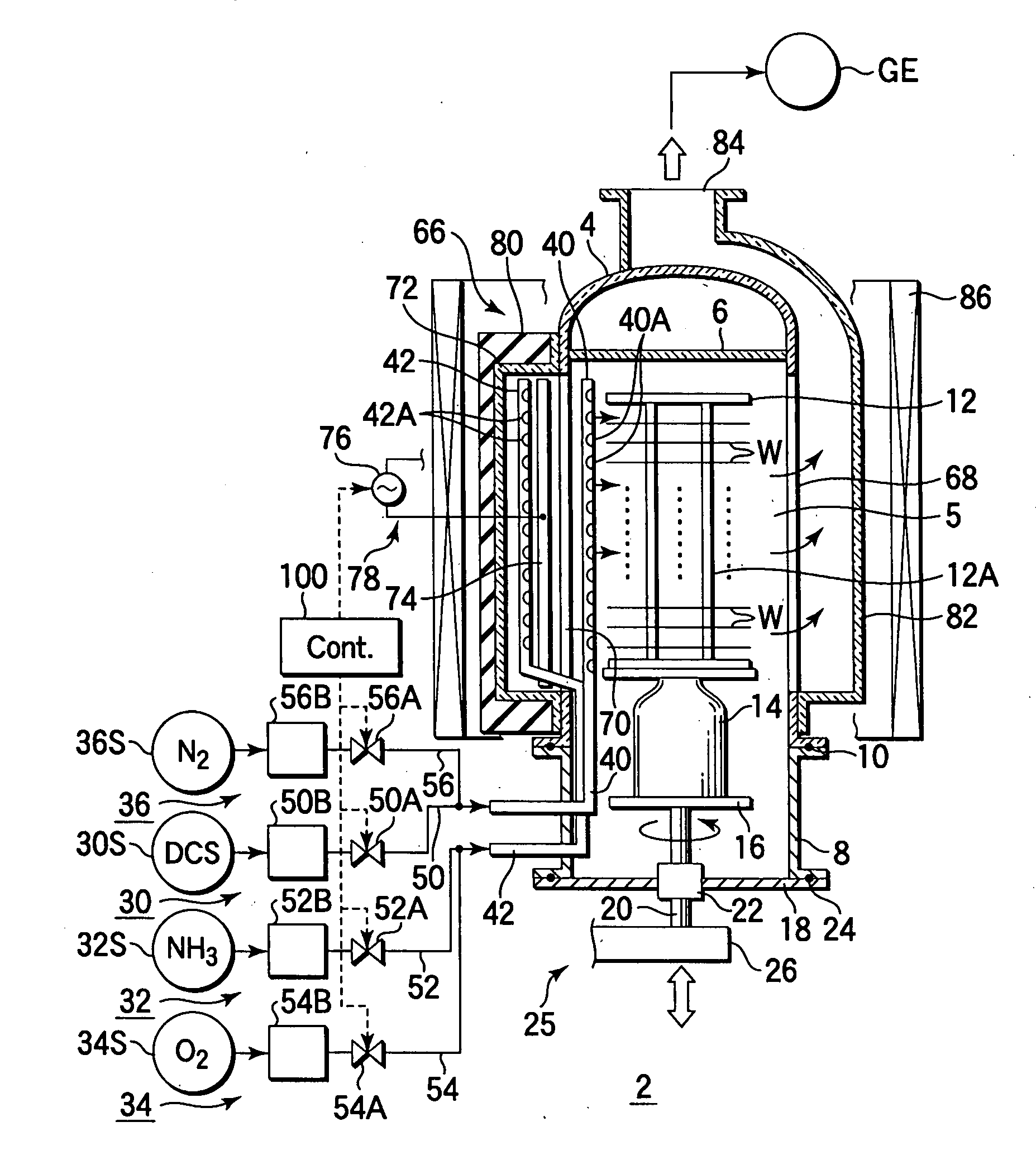
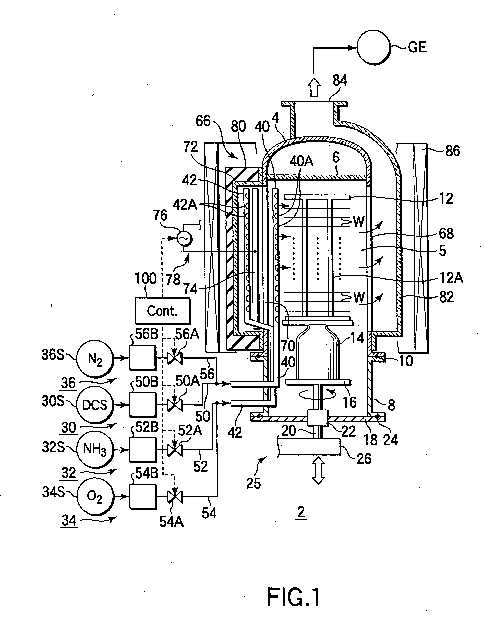
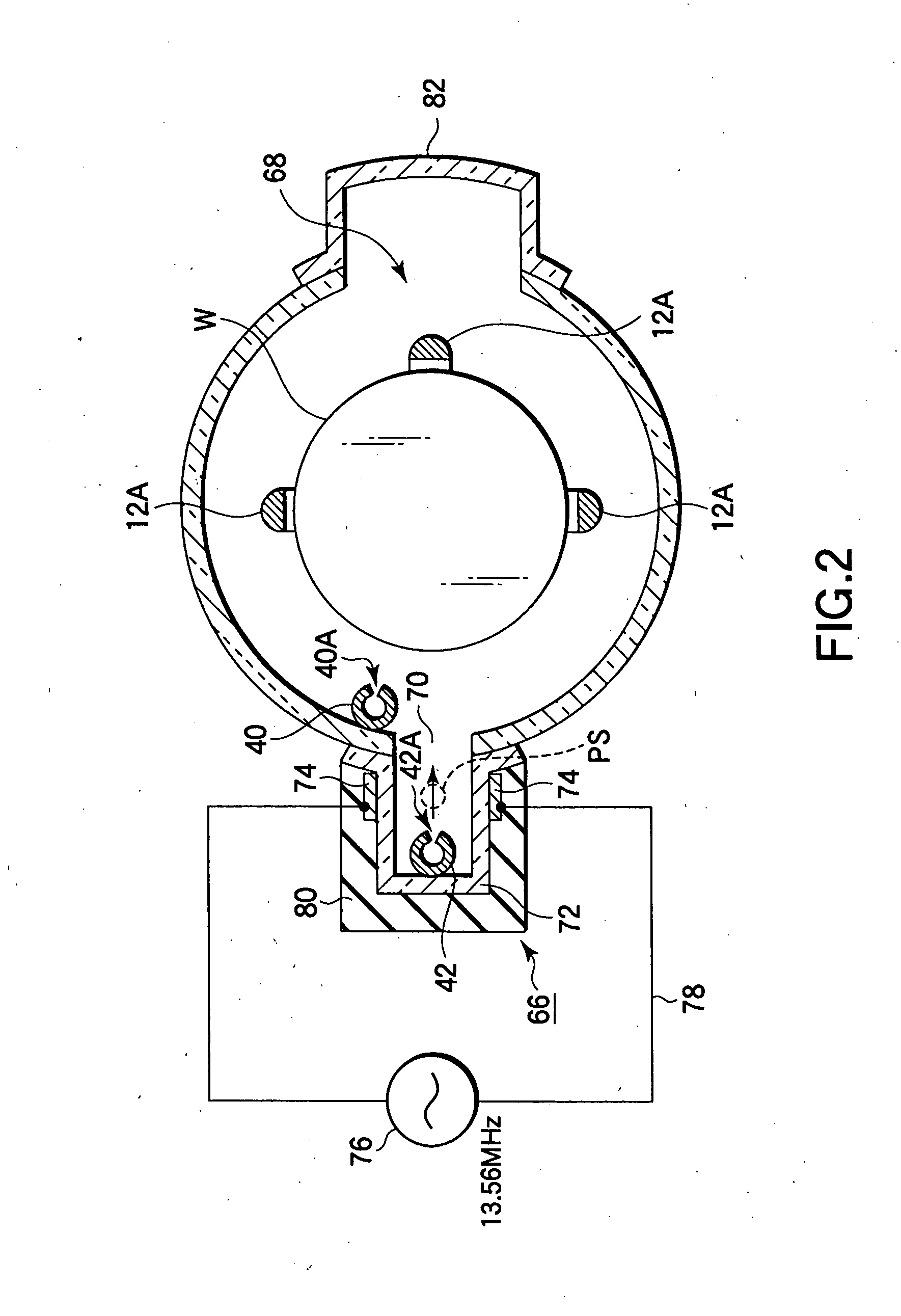
[0025]FIG. 1 is a sectional view showing a film formation apparatus (vertical CVD apparatus) according to an embodiment of the present invention. FIG. 2 is a sectional plan view showing part of the apparatus shown in FIG. 1. The film formation apparatus 2 has a process field configured to be selectively supplied with a first process gas comprising dichlorosilane (DCS: SiH2Cl2) gas as a silicon source gas, a second process gas comprising ammonia (NH3) gas as a nitriding gas, and a third process gas comprising oxygen (O2) gas as an oxidizing gas for an auxiliary process. The film formation apparatus 2 is configured to form a silicon nitride film on target substrate...
PUM
| Property | Measurement | Unit |
|---|---|---|
| inner pressure | aaaaa | aaaaa |
| depth | aaaaa | aaaaa |
| thickness | aaaaa | aaaaa |
Abstract
Description
Claims
Application Information