Heat treatment device

a treatment device and heat treatment technology, applied in the direction of heating arrangements of hot plates, lighting and heating apparatus, furniture, etc., can solve the problems of complex structure, and inability to keep line width uniform, so as to prevent warping of work substrates and perform uniform cooling processing

Active Publication Date: 2008-06-12
TOKYO ELECTRON LTD
View PDF7 Cites 28 Cited by
  • Summary
  • Abstract
  • Description
  • Claims
  • Application Information

AI Technical Summary

Benefits of technology

[0011]An object of the invention is to provide a heat treatment device that suppresses a warp of a work substrate and performs uniform cooling processing.

Problems solved by technology

Therefore, the wafer may warp due to stacking of different kinds of films and changes in temperature and the like.
For example, when a chemically amplified resist is used and the wafer warps during cooling performed after the heat treatment subsequent to the exposure, variations occur in state of temperature lowering to a temperature (e.g., 50 degrees C.) at which an acid catalytic reaction on the wafer surface stops, and a line width cannot be kept uniform.
Therefore, the structure is complicated, and further a time for suppressing the warp is required so that it is difficult to perform the cooling processing within a short time after the heat treatment.
Also, when the wafer warps into a complicated form, it is difficult to press reliably the wafer onto the projections, and it may be impossible to suppress reliably the warp of the wafer.

Method used


Image

  • Heat treatment device
  • Heat treatment device
  • Heat treatment device

Examples


first embodiment

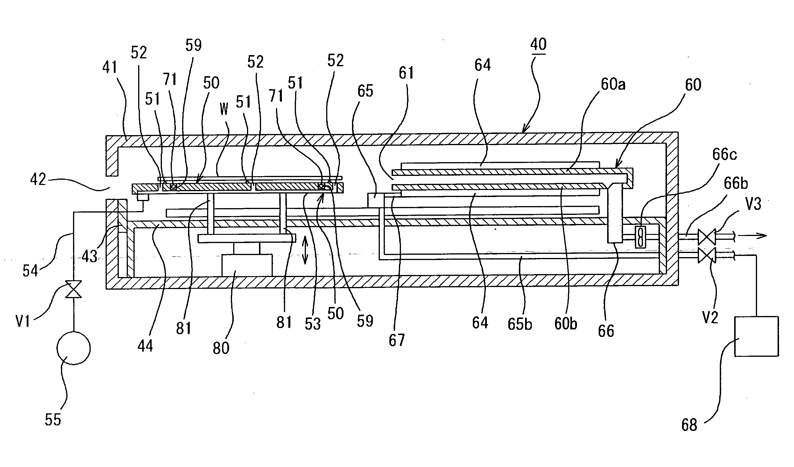
[0057]FIG. 4 is a schematic perspective view showing a major portion of a first embodiment of heat treatment device 40 according to the invention. FIG. 5 is a schematic cross section of heat treatment device 40, and FIG. 6 is a schematic plan of heat treatment device 40.

[0058]As shown in FIG. 5, heat treatment device 40 includes a casing 41 forming a processing container, and a transport opening 42 is formed for wafer W at the side wall of casing 41. Transport opening 42 can be closed by a shutter 43. When wafer W is being heater, an external air may flow into casing 41 through transport opening 42, and thereby may disturb a gas flow formed around wafer W as described later. Therefore, shutter 43 is employed for preventing this situation. However, shutter 43 may be replaced with, e.g., an air curtain formed near transport opening 42 for preventing entry of an external air.

[0059]A base 44 is arranged under casing 41. On a front side of base 44, i.e., on a side near transport opening ...

second embodiment

[0095]The first embodiment has been described in connection with the case where the coolant passage is formed by zigzag cooling pipe 58 arranged at cooling plate 50. However, cooling pipe 58 may be replaced with a flexible coolant-containing bag 90 forming a coolant passage as shown in FIGS. 9A-9C and FIGS. 10A-10C. This coolant-containing bag 90 may be made of, e.g., aluminum alloy similarly to cooling plate 50 of the first embodiment, and may be layered over a cooling plate body 500 of a substantially circular plate-like form having substantially the same diameter as wafer W to form a cooling plate 50A. In this case, coolant-containing bag 90 is provided with a plurality of (e.g., nine) suction holes 52 located, e.g., at the center of cooling plate 50A and circumferentially equally spaced eight positions on the same circle. Also, each suction hole 52 is connected to vacuum pump 55. Thereby, the negative pressure produced by vacuum pump 55 can act on a portion near each suction hol...

third embodiment

[0101]FIG. 13 is a schematic plan showing a major portion of a third embodiment of the heat treatment device according to the invention, and FIG. 14 is a schematic cross section of the heat treatment device of the third embodiment.

[0102]A heat treatment device 40B of the third embodiment has a cooling plate 50B that is made of aluminum alloy similarly to the first embodiment and has a function of transferring wafer W. similarly to the first embodiment. As shown in FIG. 13, heat treatment device 40B includes a plate moving mechanism 100 that can move cooling plate 50B into and from heating chamber 60 and is formed of, e.g., a ball screw mechanism, a timing belt mechanism or the like. Heat treatment device 40B also includes insertion open grooves 501 and 502 for avoiding interface with vertically movable support pins 201 that transfer wafer W to and from cooling plate 50.

[0103]In this structure, cooling plate 50B includes two insertion open grooves 501 and 502 having different lengths...


PUM


Abstract

In a heat treatment device including a heating chamber having a heating plate heating a semiconductor wafer, a cooling plate cooling the wafer heated by the heating chamber, and a transporting device transporting the wafer into and from the heating chamber, the cooling plate is provided with a coolant passage, a plurality of projections carrying the wafer with a space between the wafer and the surface of the cooling plate, and suction holes neighboring to the respective projections and connected to a suction device.

Description

BACKGROUND OF THE INVENTION[0001]1. Field of the Invention[0002]The invention relates to a heat treatment device, and particularly to a heat treatment device performing heat treatment on a work substrate (i.e., a substrate to be treated) such as a semiconductor wafer or an LCD substrate.[0003]2. Description of the Background Art[0004]In a conventional photoresist step, which is one of semiconductor manufacturing steps, resist is applied over a surface of a semiconductor wafer or a substrate of an LCD substrate or the like (which will be referred to as a “wafer” hereinafter), and is exposed with a predetermined pattern. Then, a developer liquid is supplied onto the surface of the wafer, and development is performed to form a resist pattern. For protecting the resist, a step of applying a protective film over the surface of a resist layer is generally incorporated into the above photoresist step.[0005]In recent years, it has been increasingly requested to increase an exposure resoluti...

Claims


Application Information

Patent Timeline
Patent Type & Authority Applications(United States)
IPC IPC(8): F25B29/00
CPCF28D15/00H01L21/67109F28F3/12F28D15/0266
Inventor FUKUOKA, TETSUOKITANO, TAKAHIROTERADA, KAZUO
Owner TOKYO ELECTRON LTD
Why Eureka
Try Eureka