Supercharge Your Innovation With Domain-Expert AI Agents!

Controlled nanowire in permanent integrated nano-templates and method of fabricating sensor and transducer structures

a technology of controlled nanowires and integrated nano-templates, which is applied in the field of controlled nanowires in permanent integrated nano-templates and the method of fabricating sensor and transducer structures, can solve the problems of nanowires produced, difficult to assemble wires into rational device geometries, and excluding the opportunity for nanoscale phenomena such as quantum confinemen

Inactive Publication Date: 2008-06-12
FONASH STEPHEN +7
View PDF6 Cites 12 Cited by
  • Summary
  • Abstract
  • Description
  • Claims
  • Application Information

AI Technical Summary

Benefits of technology

This approach enables the precise control of nanostructure growth, integration into device structures, and elimination of the need for post-synthesis assembly, facilitating the creation of complex devices like transducers and sensors with enhanced control over nanowire dimensions and orientation.

Problems solved by technology

It remains a challenge to grow composition-controllable, orientation-controllable and size-controllable nanowires.
It is also difficult to assemble the wires into rational device geometries and enable current flow between nanoscale and microscale structures.
The use of the alumina membranes as the templates (e.g., dissolved / etched away templates) may provide control over nanowire diameter and length while also enabling the production of single crystal material, however, there are many disadvantages to current approaches.
1. Due to the use of pre-formed commercial templates, the diameter of nanowires produced with this method is relatively large (usually 200 nm) and precludes the opportunity for nanoscale phenomena such as quantum confinement;
These channels are not very straight or uniform;
All of these steps use electroplating and make the process complicated;
5. The alumina template is disposed of (etched away) in this approach and cannot be integrated with device assembly.
It is very difficult to separate, move, electrically contact, if needed, and assemble these freed nanowires; and
6. The process is not compatible with on-chip fabrication and assembly, and requires post synthesis assembly of nanostructures to form more complicated devices.

Method used


Image

  • Controlled nanowire in permanent integrated nano-templates and method of fabricating sensor and transducer structures
  • Controlled nanowire in permanent integrated nano-templates and method of fabricating sensor and transducer structures
  • Controlled nanowire in permanent integrated nano-templates and method of fabricating sensor and transducer structures

Examples


Embodiment Construction

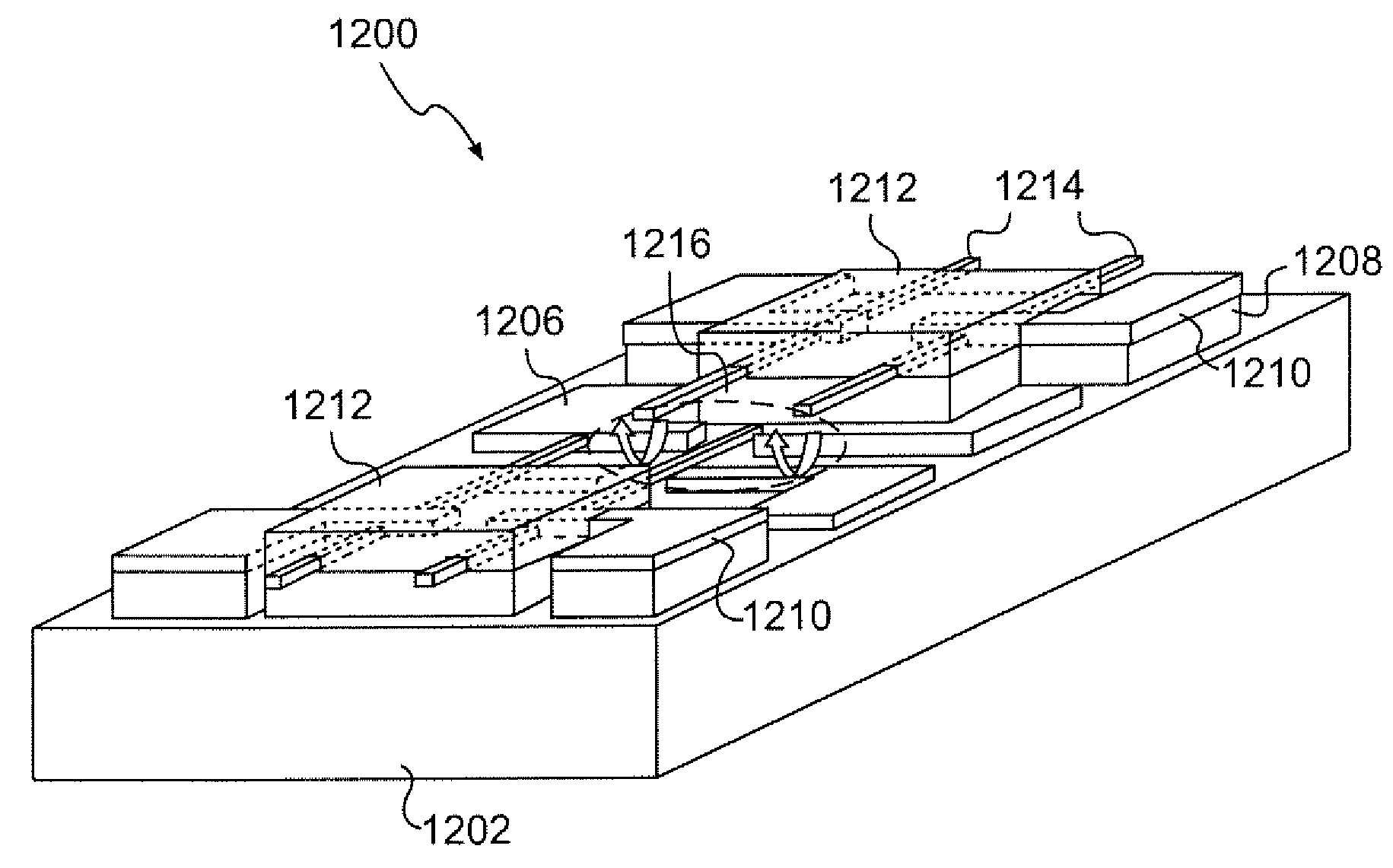
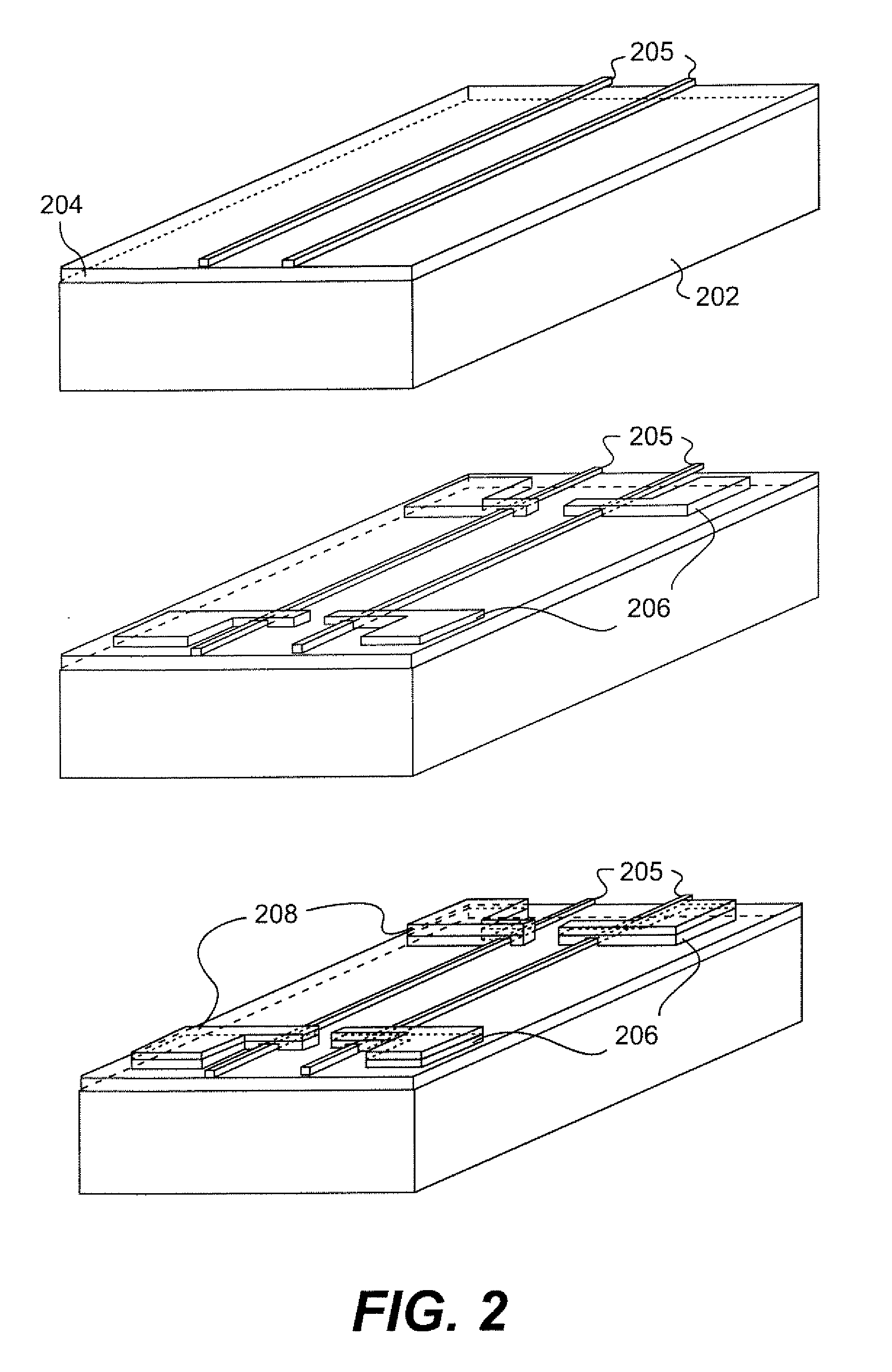
[0047]This invention presents a novel method to form uniform or heterogeneous, straight or curved and size-controllable nanostructures including, for example, nanowires, nanoribbons, nanotubes, and nanotapes (e.g., high width to height ratio cross-section) including single crystal SiNW, in a nanochannel template. In the case of semiconductor nanowires, doping can be included during growth. Electrode contacts are present as needed and may be built in to the template structure. Thus, completed devices such as diodes, transistors, solar cells, sensors, and transducers are fabricated, contacted, and arrayed as nanostructure and resultant device fabrication is completed. Optionally, the template is not removed and may become part of the structure.

[0048]Nanochannel templates are fabricated by the combined use of lithography and sacrificial material patterning techniques known in the art. The nanochannels can be straight or curved, as desired, and the sizes are controllable. Hence the nano...


PUM

PropertyMeasurementUnit
diameteraaaaaaaaaa
critical diameteraaaaaaaaaa
sizeaaaaaaaaaa

Abstract

This invention presents a novel method to form uniform or heterogeneous, straight or curved and size-controllable nanostructures including, for example, nanotubes, nanowires, nanoribbons, and nanotapes, including SiNW, using a nanochannel template. In the case of semiconductor nanowires, doping can be included during growth. Electrode contacts are present as needed and may be built in to the template structure. Thus completed devices such as diodes, transistors, solar cells, sensors, and transducers are fabricated, contacted, and arrayed as nanowire or nanotape fabrication is completed. Optionally, the template is not removed and may become part of the structure. Nanodevices such as nanotweezers, nanocantilevers, and nanobridges are formed utilizing the processes of the invention.

Description

RELATED APPLICATION DATA[0001]This application is a divisional of U.S. patent application Ser. No. 11 / 008,989, filed Dec. 13, 2004, which claims the benefit of U.S. Provisional Patent Application No. 60 / 528,487, filed on Dec. 11, 2003, both of which are hereby incorporated by reference for all purposes as if fully set forth herein.BACKGROUND OF THE INVENTION[0002]1. Field of the Invention[0003]The present invention relates to a method to form uniform or heterogeneous, straight or curved and size-controllable nanostructures using nanochannel templates. More specifically, this method may be used to form devices and systems utilizing nanowires.[0004]2. Discussion of the Related Art[0005]One-dimensional metallic and semiconducting nanowires have attracted much attention recently owing to their fundamental and technological importance. Much of this attention is focused on Si nanowires (SiNW) since, at this scale, Si can become a direct-band-gap material. In the article, by B. Marsen, et ...

Claims


Application Information

Patent Timeline
Patent Type & Authority Applications(United States)
IPC IPC(8): H01L29/06B81C1/00H01L21/20H01L21/44H10K99/00
CPCB81B2203/0109Y02E10/549B81C1/0019B82Y10/00H01L21/0237H01L21/02532H01L21/0259H01L21/02603H01L21/02639H01L21/02645H01L21/02653H01L29/0665H01L29/0673H01L29/068H01L51/0002Y10S977/762B81B2203/0118H10K71/10
Inventor FONASH, STEPHENSHAN, YINGHUIPENG, CHIH-YIKALKAN, ALI KAANCUIFFI, JOSEPH D.HAYES, DANIELBUTTERFOSS, PAULNAM, WOOK JUN
Owner FONASH STEPHEN
Features
  • R&D
  • Intellectual Property
  • Life Sciences
  • Materials
  • Tech Scout
  • Unparalleled Data Quality
  • Higher Quality Content
  • 60% Fewer Hallucinations
Learn More