Nonvolatile semiconductor storage device and manufacturing method of the same

Active Publication Date: 2008-06-19
RENESAS ELECTRONICS CORP
View PDF19 Cites 18 Cited by
  • Summary
  • Abstract
  • Description
  • Claims
  • Application Information

AI Technical Summary

Benefits of technology

[0029]An object of the present invention is to provide a technology capable of improving the reliability of a nonvolatile semiconductor storage device.
[0030]Fur

Problems solved by technology

However, in the memory cell array described in the Patent Document 2 in which a silicon nitride film to be the charge trapping layer is present in the element isolation region, the problems as follows may occur when miniaturization further progresses in the future.
Further, since the charge trapping layer is formed also in the element isolation region, charges such as electrons and holes held in the charge trapping layer in the element formation region are adversely diffused via the charge trapping layer in the element isolation region in the data holding operation.
Conse

Method used


Image

  • Nonvolatile semiconductor storage device and manufacturing method of the same
  • Nonvolatile semiconductor storage device and manufacturing method of the same
  • Nonvolatile semiconductor storage device and manufacturing method of the same

Examples


first embodiment

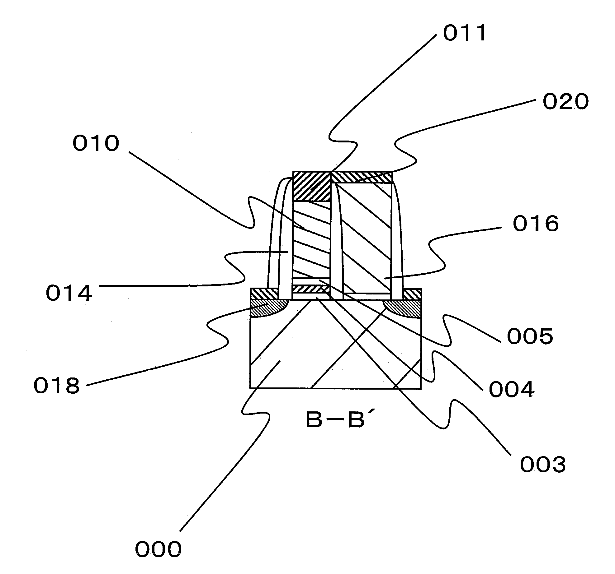
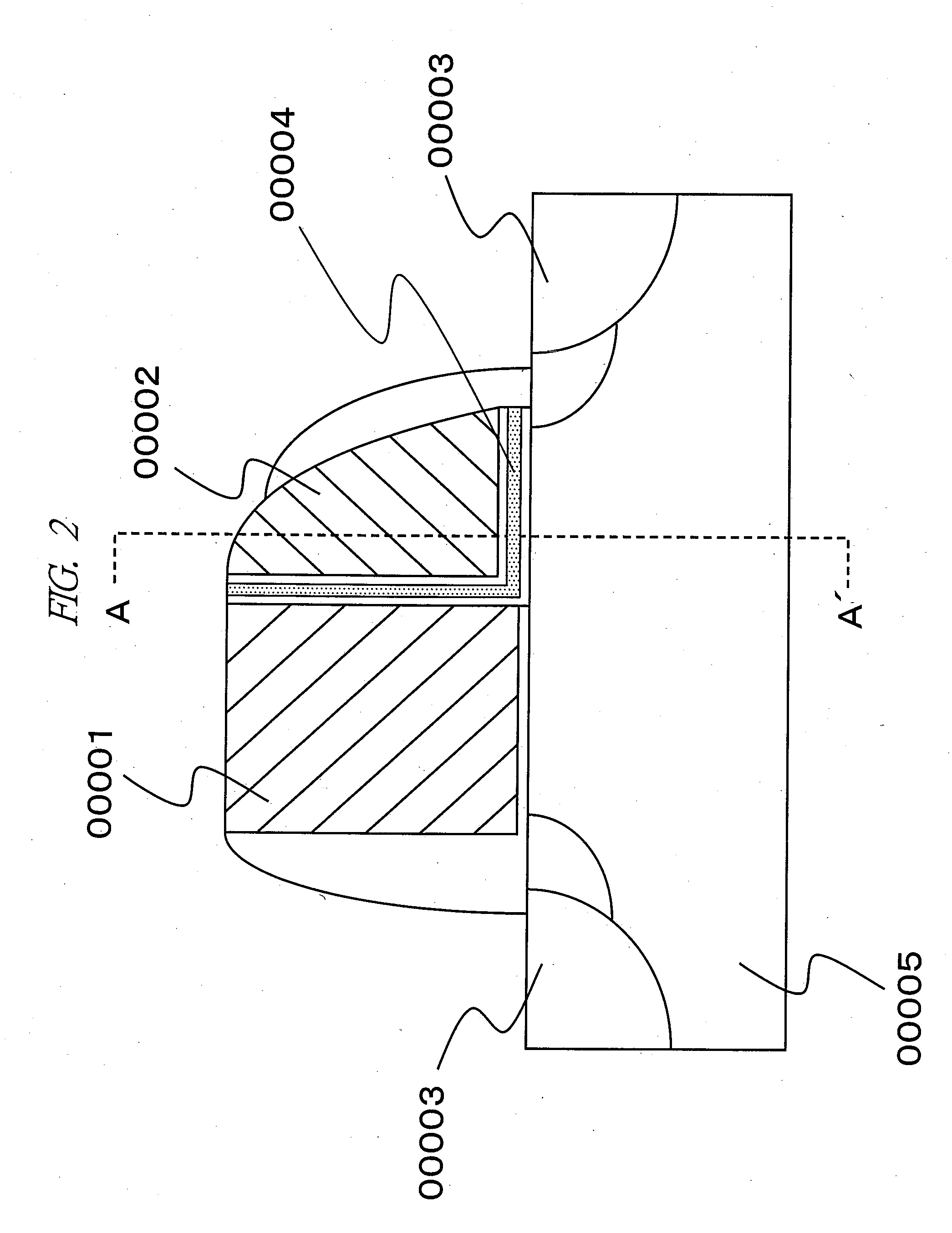
[0097]FIG. 4 is a plan view of a part of a semiconductor substrate showing an example of a memory cell region in a nonvolatile semiconductor storage device according to the first embodiment. In an element isolation region extending in a lateral direction on surface of a silicon substrate (semiconductor substrate) 000, an element isolation insulating film 009 extending in the lateral direction is formed to prevent the current interference between memory cells adjacent in a longitudinal direction. Also, the region other than that is an element formation region, and a memory cell, a source line and a bit line are formed therein. Further, a gate electrode 010 of a memory transistor (hereinafter, referred to as memory gate or memory gate electrode) extends thereon in the longitudinal direction, and a gate electrode 016 of a selection transistor (hereinafter, referred to as selection gate or selection gate electrode) extends in the longitudinal direction so as to be adjacent to the memory...

second embodiment

[0126]FIG. 29 is a cross-sectional view showing a nonvolatile semiconductor integrated storage device according to the second embodiment. The difference between the memory cell structure of the second embodiment and that of the first embodiment lies in that the selection gate electrode 016 is formed by the sidewall process. By forming the selection gate electrode 016 as the sidewall, the effect of reducing the memory cell area can be achieved in addition to those of the first embodiment.

third embodiment

[0127]FIG. 30 is a plan view of a part of a semiconductor substrate showing an example of a nonvolatile semiconductor storage device according to the third embodiment in the same manner as FIG. 4 of the first embodiment described above. FIG. 31, FIG. 32 and FIG. 33 are cross-sectional views of the semiconductor substrate each taken along the lines A-A′, B-B′ and C-C′ in FIG. 30. Also, FIG. 34 is a plan view showing an example of the peripheral circuit region of the same device, and FIG. 35 is a cross-sectional view taken along the line D-D′ in FIG. 34. More specifically, the regions represented by the lines A-A′, B-B′ and C-C′ correspond to the cross-sectional views of the memory cell region and the region represented by the line D-D′ corresponds to the cross-sectional view of the peripheral circuit region. The difference between the third embodiment and the first embodiment lies in that the memory gate electrodes are united by the polysilicon film at a position higher than the uppe...


PUM


Abstract

A charge trapping layer in an element isolation region and that in an isolation region between a memory transistor and a selection transistor are removed so that the charges are not injected or trapped in the regions. Also, in an element isolation region, gate electrodes of each memory transistor are united at a position higher than a gate electrode of the selection transistor from a surface of a silicon substrate in an element isolation region, thereby reducing the capacitance between the memory transistor and the selection transistor.

Description

CROSS-REFERENCE TO RELATED APPLICATION[0001]The present application claims priority from Japanese Patent Application No. JP 2006-338386 filed on Dec. 15, 2006, the content of which is hereby incorporated by reference into this application.TECHNICAL FIELD OF THE INVENTION[0002]The present invention relates to a nonvolatile semiconductor storage device. More particularly, it relates to a technology effective for achieving the high reliability and the high-speed operation of a MONOS (metal oxide nitride oxide semiconductor) memory cell.BACKGROUND OF THE INVENTION[0003]A nonvolatile memory is known as one of the integrated semiconductor memories incorporated in an LSI. This is the element in which stored information is not lost even when the power of the LSI is turned off and is an extremely important element for using the LSI in the various applications. Information can be stored in the nonvolatile memory by various methods. As the nonvolatile memories in which information is stored by...

Claims


Application Information

Patent Timeline
IPC IPC(8): H01L29/792H01L21/336
CPCG11C16/0466H01L27/115H01L29/7851H01L27/11524H01L27/11521H10B69/00H10B41/30H10B41/35
Inventor ARIGANE, TSUYOSHIHISAMOTO, DIGHSHIMAMOTO, YASUHIRO
Owner RENESAS ELECTRONICS CORP
Why Eureka
Try Eureka