Semiconductor Photodiode and Method of Making

a technology of semiconductors and photodiodes, applied in the field of semiconductor photodiodes, can solve the problems of small high cost, and large volume of products, and achieve the effect of improving the fill factor of photodiodes and reducing the cost of production

Inactive Publication Date: 2008-06-26
ECOLE POLYTECHNIQUE FEDERALE DE LAUSANNE (EPFL)
View PDF5 Cites 21 Cited by
  • Summary
  • Abstract
  • Description
  • Claims
  • Application Information

AI Technical Summary

Benefits of technology

[0010]In the following the term “avalanche photodiode” means a diode formed as a pn-junction between n-type semiconductor material and p-type semiconductor material and operated biased with a reverse voltage for making use of the avalanche effect. The avalanche effect consists in that

Problems solved by technology

The main drawback of these devices is their incompatibility with standard electronics which results in bulky and expensive products.
However, these photodiodes, although being compatible with the well-known and widespread CMOS technologies, require custom process stages and extra masks.
The drawback of this photodiode is its small fill factor as a result of the complex guard ring structure.
In addition, the leakage current is too high, which limits the

Method used


Image

  • Semiconductor Photodiode and Method of Making
  • Semiconductor Photodiode and Method of Making
  • Semiconductor Photodiode and Method of Making

Examples


Embodiment Construction

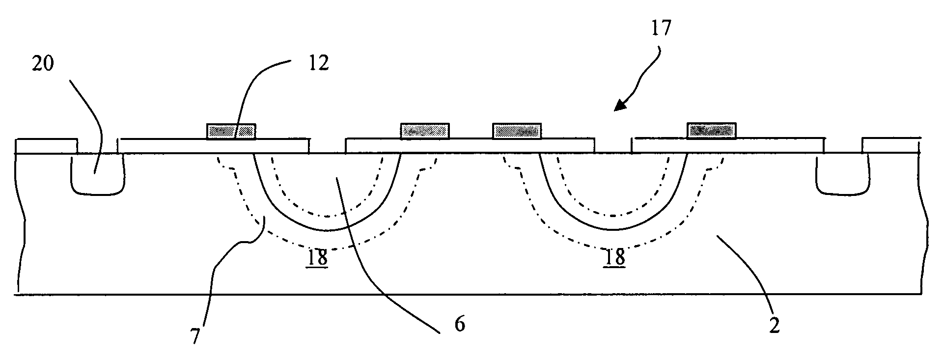
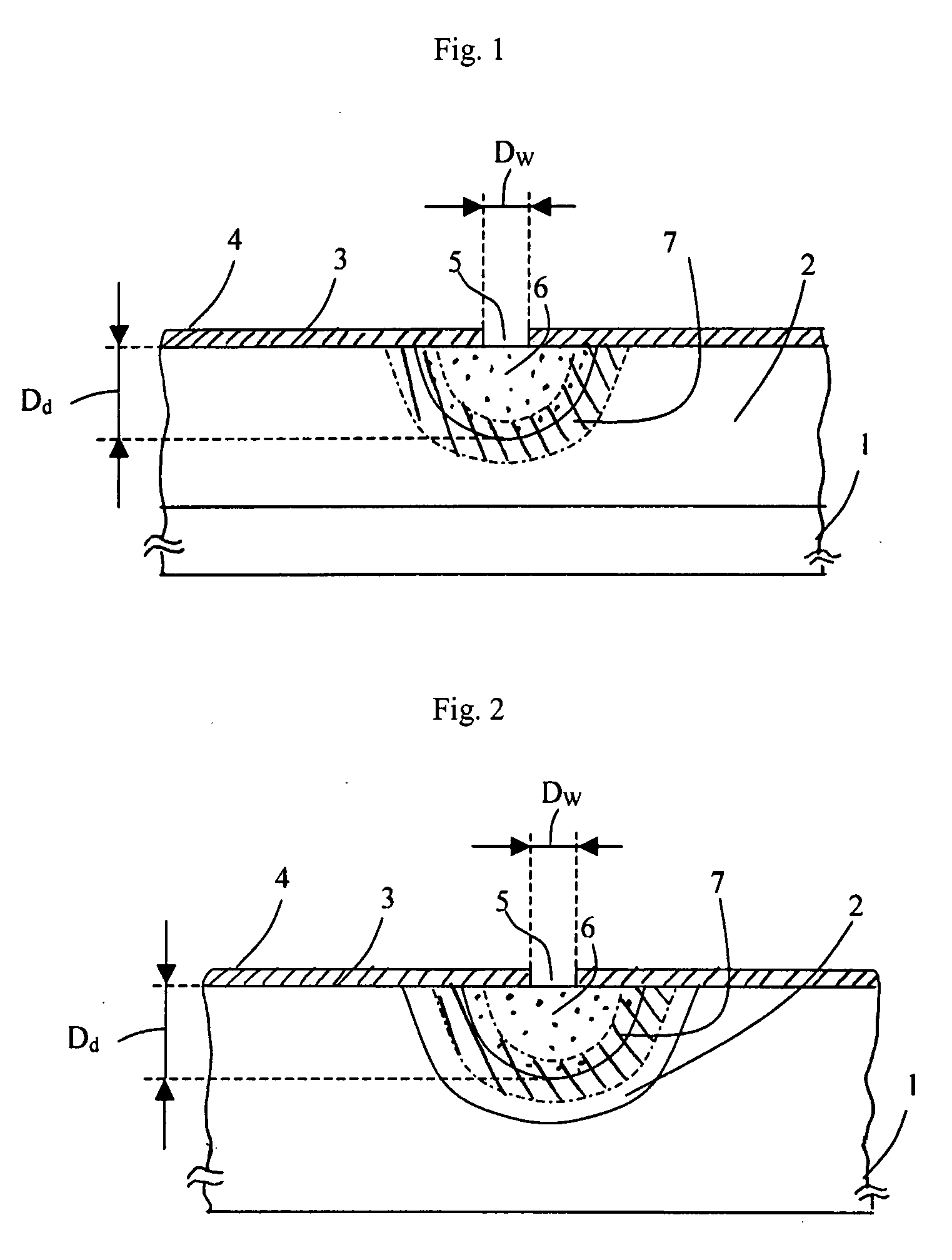
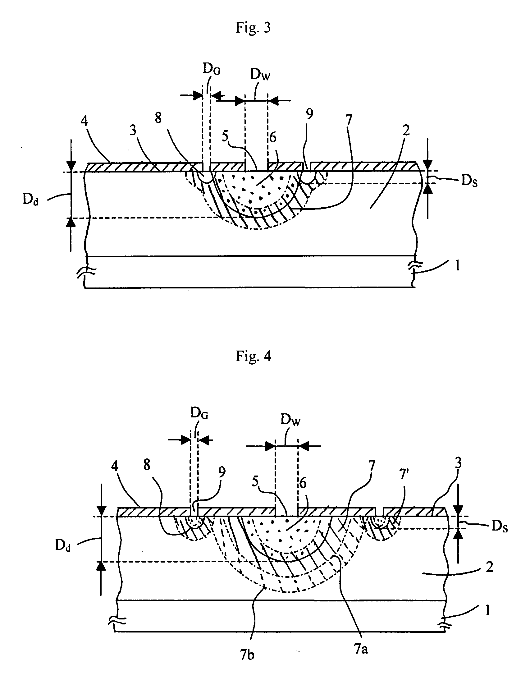
[0030]The photodiode according to the invention has a unique structure designed with the intention to achieve the same electrical field throughout the whole pn-junction so that breakdown occurs with the same probability at any place of the pn-junction. This is achieved with a three dimensionally symmetrical structure, namely a hemispherical structure. The photodiode is preferably manufactured in a standard CMOS technology having high voltage capability. Such a CMOS technology comprises p-doped and / or n-doped regions with deep diffusion of e.g. 5 micrometers or a for example epitaxially grown layer of approximately uniform doping. FIG. 1 illustrates the process steps for making a pn-junction having approximately this structure.

[0031]FIG. 1 shows a cross section of a semiconductor wafer 1. The semiconductor wafer 1 or at least a region 2 or layer below the surface 3 of the wafer 1 consists of semiconductor material of a first conductivity type. Preferably, the doping and hence conduct...


PUM


Abstract

A semiconductor photodiode (18) is formed as a pn-junction between a region (2) of a first conductivity type and a region (6) of a second conductivity type. The region (6) of the second conductivity type is approximately hemispherical. A mini guard ring (8), i.e. a ring of the second conductivity type having a junction depth that is much smaller than the junction depth of the region (6) preferably surrounds the region (6) in order to prevent surface trapping. The photodiode (18) is operated with a high reverse bias so that light falling on the photodiode (18) produces the avalanche effect.

Description

CROSS REFERENCE TO RELATED APPLICATION[0001]The present application claims priority of European patent application number 05100128.7 of ECOLE POLYTECHNIQUE FEDERALE DE LAUSANNE entitled Semiconductor photodiode and method of making filed on Jan. 11, 2005. The present application is further related to and claims priority of PCT application number PCT / EP2006 / 050103 of ECOLE POLYTECHNIQUE FEDERALE DE LAUSANNE entitled Semiconductor photodiode and method of making, filed on Jan. 10, 2006, the disclosure of which is herein incorporated by reference.FIELD OF THE INVENTION[0002]The invention concerns a semiconductor photodiode for the detection of photons or light and a process for making a semiconductor photodiode.BACKGROUND OF THE INVENTION[0003]A diode is formed between two areas of semiconductor material of different conductivity type, namely p-type material and n-type material. Besides many other applications, diodes can be used for the detection of photons or light and are widely use...

Claims


Application Information

Patent Timeline
IPC IPC(8): H01L31/0352H01L31/18
CPCH01L31/101H01L27/146H01L31/107H01L31/03529H01L27/1446
Inventor POPOVIC, RADIVOJEXIAO, ZHEN
Owner ECOLE POLYTECHNIQUE FEDERALE DE LAUSANNE (EPFL)
Why Eureka
Try Eureka