Double-Side-Bias Methods of Programming and Erasing a Virtual Ground Array Memory

Inactive Publication Date: 2008-06-26
MACRONIX INT CO LTD
View PDF9 Cites 4 Cited by
  • Summary
  • Abstract
  • Description
  • Claims
  • Application Information

AI Technical Summary

Benefits of technology

[0009]The present invention describes methods for applying a double-side-bias (DSB) operation to a virtual ground array memory composed of a matrix of N-bit memory cells. In a first embodiment, the virtual ground array is programmed by a double-side-bias method which applies the same or similar biasing voltages simultaneously on the source region and drain region of a selected charge trapping memory cell so that the left bit and the right bit of the selected charge trapping memory cell are programmed together. A negative gate voltage, −Vg, is applied to a gate terminal of the selected charge trapping memory cell to enhance the hole injection efficiency.
[0010]In a second embodiment, the virtual ground array is erased by a double-side-bias method which applies the same or similar biasing voltages simultaneously to source regions and regions of a plurality of charge trapping memory cells in the virtual ground array so that the left bit and the right bit for each charge trapping memory cell are erased together. The double-side-bias methods in the first and second embodiments emulate plus and minus Fowler-Nordheim operations with lower bias voltages. A positive gate voltage, +Vg, is applied to a gate terminal of the selected charge trapping memory cell to enhance the electron injection efficiency.
[0012]The double-side-bias erase operation can increase the erase efficiency on the virtual ground array. The double-side-bias erase operation can also be used to obtain a sector erase on the virtual ground array. The double-side-bias method in the present invention can further be used to replace the BTBHH erase method for increasing N-bit erase efficiency on a virtual ground array.

Problems solved by technology

However, the hot hole injection causes oxide damage, leading to charge loss in the high threshold cell and charge gain in the low threshold cell Moreover, the erase time must be increased gradually during program and erase cycling due to the hard-to-erase accumulation of charge in the charge trapping structure.
This difference in erase speed results in a large Vt distribution of the erase state, where some of the cells become hard to erase and some of them are over-erased.
Thus the target threshold Vt window is closed after many program and erase cycles and poor endurance is observed.
This phenomenon will become more serious as the technology continues scaling down.

Method used


Image

  • Double-Side-Bias Methods of Programming and Erasing a Virtual Ground Array Memory
  • Double-Side-Bias Methods of Programming and Erasing a Virtual Ground Array Memory
  • Double-Side-Bias Methods of Programming and Erasing a Virtual Ground Array Memory

Examples


Embodiment Construction

[0022]A description of structural embodiments and methods of the present invention is provided with reference to FIGS. 1-7. It is to be understood that there is no intention to limit the invention to the specifically disclosed embodiments, but that the invention may be practiced using other features, elements, methods and embodiments. Like elements in various embodiments are commonly referred to with like reference numerals.

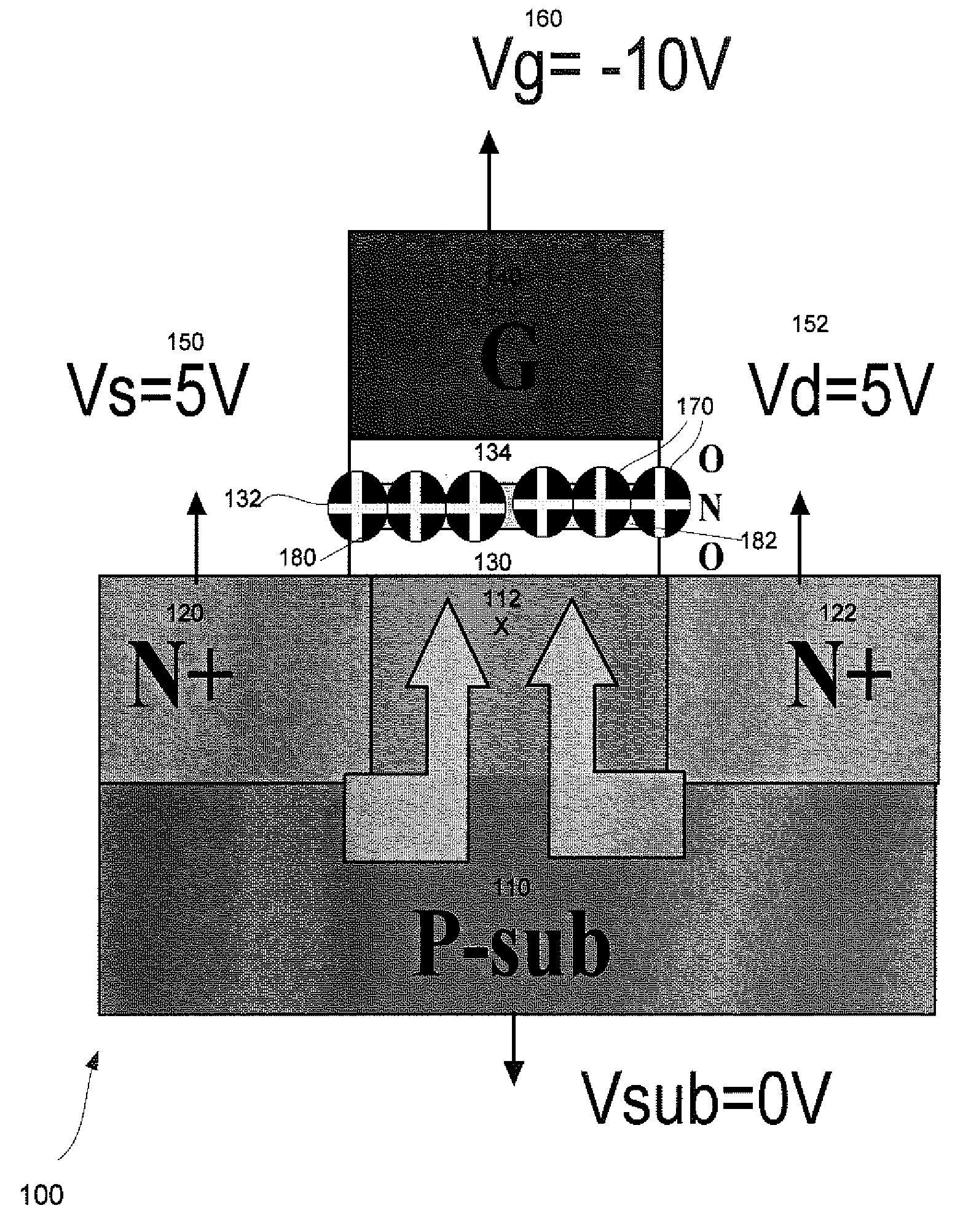
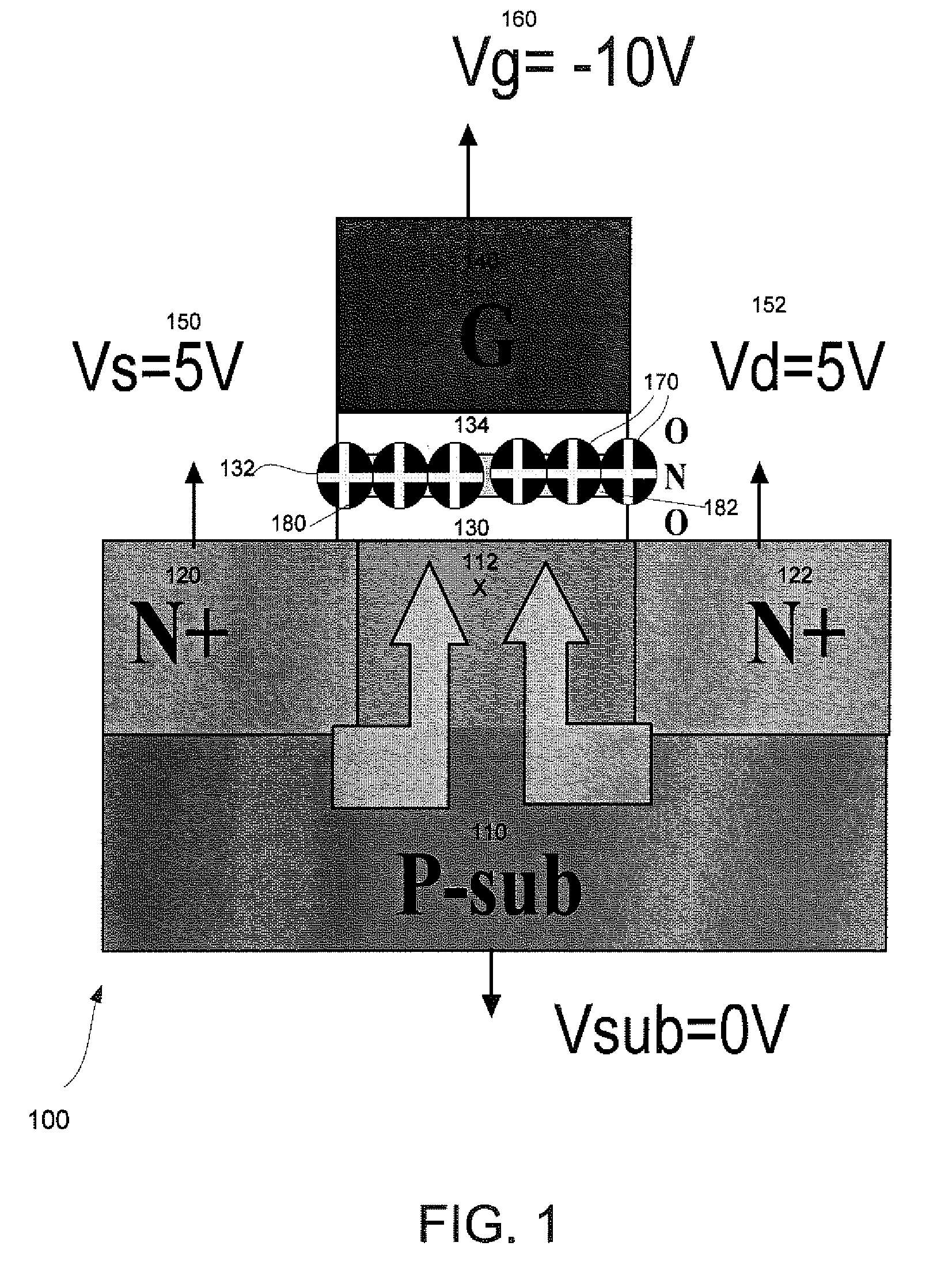
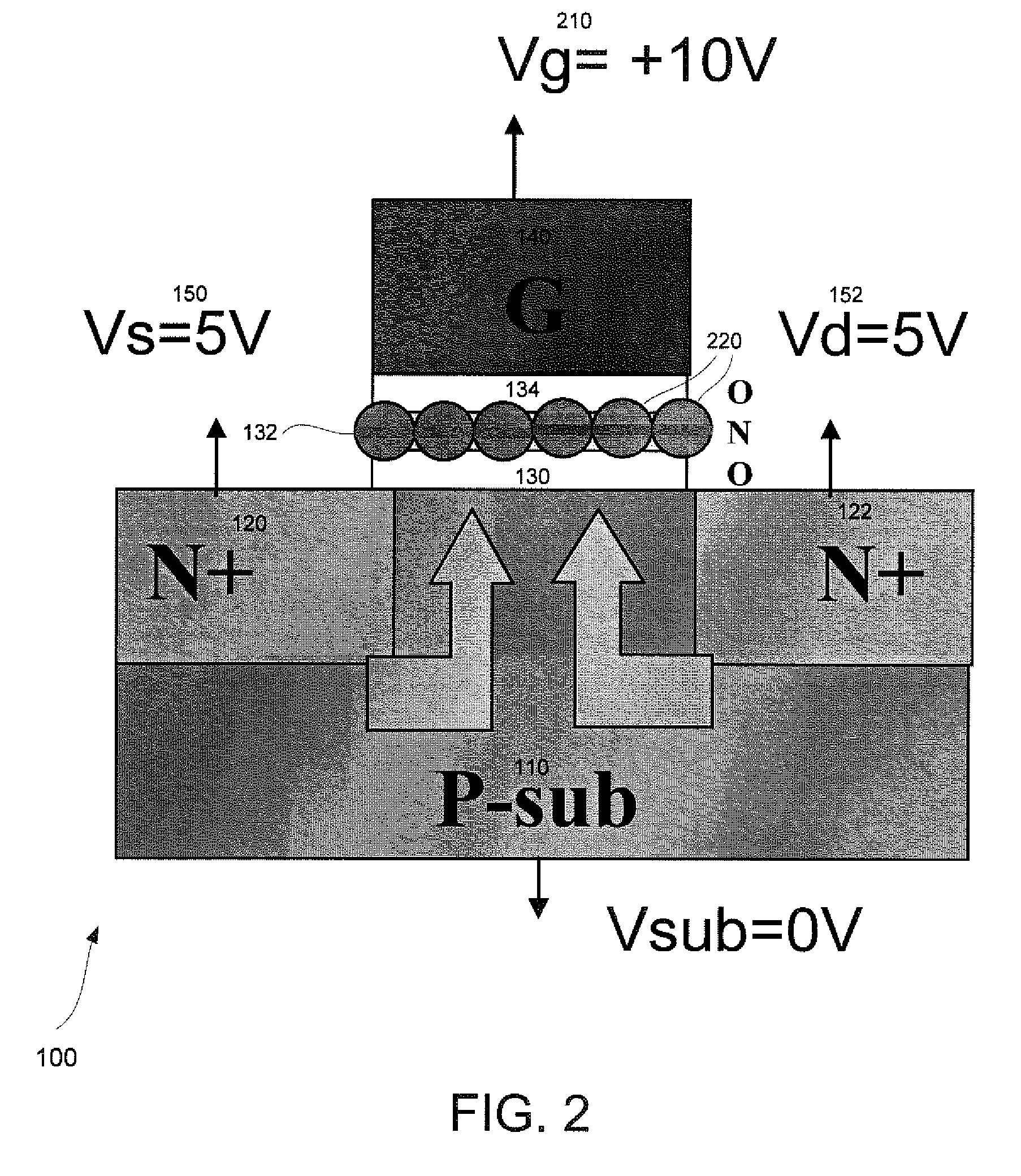
[0023]FIG. 1 is a process diagram illustrating a cross-sectional view of erasing a charge trapping memory cell (or N-bit) 100 by using a double-side-bias (DSB) hole-injection (HI) method. The charge trapping memory cell 100 comprises a p-substrate 110 with n+ doped regions 120 and 122, and a p-doped region between the n+ doped regions 120 and 122. A channel width X 112 of the p-substrate 110 is positioned between the n+ doped region 120 on the left end and the n+ doped region 122 on the right end. A bottom dielectric structure 130 (bottom oxide) overlays a top su...


PUM


Abstract

The present invention provides a method for applying a double-side-bias operation to a virtual ground array memory composed of a matrix of N-bit memory cells. In a first embodiment, the virtual ground array is programmed by a double-side-bias method which applies the same or similar biasing voltage simultaneously on the source region and drain region of a selected charge trapping memory cell so that the left bit and the right bit of the selected charge trapping memory cell are programmed together. In a second embodiment, the virtual ground array is erased by a double-side-bias method which applies the same or similar biasing voltage simultaneously on source regions and regions of a plurality of charge trapping memory cells in the virtual ground array so that the left bit and the right bit of each charge trapping memory cell are erased together.

Description

BACKGROUND OF THE INVENTION[0001]1. Field of the Invention[0002]The present invention relates generally to electrically programmable and erasable memory and more particularly to programming and erasing of a charge trapping memory array.[0003]2. Description of Related Art[0004]Electrically programmable and erasable nonvolatile memory technologies based on charge storage structures known as Electrically Erasable Programmable Read-Only Memory (EEPROM) and flash memory are used in a variety of modern applications. A flash memory is designed with an array of memory cells that can be independently programmed and read. Sense amplifiers in a flash memory are used to determine the data value or values stored in a nonvolatile memory. In a typical sensing scheme, an electrical current through the memory cell being sensed is compared to a reference current by a current sense amplifier.[0005]A number of memory cell structures are used for EEPROM and flash memory. As the dimensions of integrated ...

Claims


Application Information

Patent Timeline
IPC IPC(8): G11C16/14
CPCG11C16/0491G11C16/0475
Inventor WU, CHAO-I
Owner MACRONIX INT CO LTD
Why Eureka
Try Eureka