Method, system, and computer program product for preparing multiple layers of semiconductor substrates for electronic designs

a technology of electronic designs and semiconductor substrates, applied in semiconductor/solid-state device testing/measurement, individual semiconductor device testing, instruments, etc., can solve the problems of affecting the interconnection performance, requiring more yet smaller transistors to be closely packed, and more functionality and higher performan

Active Publication Date: 2008-07-03
CADENCE DESIGN SYST INC
View PDF25 Cites 64 Cited by
  • Summary
  • Abstract
  • Description
  • Claims
  • Application Information

AI Technical Summary

Benefits of technology

[0011]Thus, there exists a need for an improved method for producing a multiple le

Problems solved by technology

The ever-growing demand for more functionality and higher performance has caused increased complexity in integrated circuit (IC) designs requiring more yet smaller transistors to be closely packed.
This continual demand for smaller features improves the performance of integrated circuits but also adversely impacts the interconnect performances.
Smaller wire sizes and spacing and longer lines to traverse larger chip areas have increased the resistance, capacitance and, as a result, the R-C delay.
Moreover, this interconnect delay becomes more significant and can no longer be ignored as the feature sizes continue to shrink into the deep submicron regime.
Another adverse impact of this continual increase in chip size as a result of the demand for more functionality and higher performance is the number of chips per wafer decreases and thus increases the manufacturing cost as well as the cost of ownership of integrated circuits.
Several approaches have been investigated, yet various limitations have been identified for each approach.
However, the limitation on this method is the precision, or lack thereof, of overlaying two processed wafers each of which has been manufactured with extremely high precision atop each other.
Typically, the best alignment techniques today may only bring the two wafers within +/−2 microns, which is far less precise than what is required for integrated circuits.
Such an misalignment may cause great difficulties in the interconnects between the two pieces of wafers being bonded or glued together.
Moreover, the variation in the flatness of the p

Method used


Image

  • Method, system, and computer program product for preparing multiple layers of semiconductor substrates for electronic designs
  • Method, system, and computer program product for preparing multiple layers of semiconductor substrates for electronic designs
  • Method, system, and computer program product for preparing multiple layers of semiconductor substrates for electronic designs

Examples


Embodiment Construction

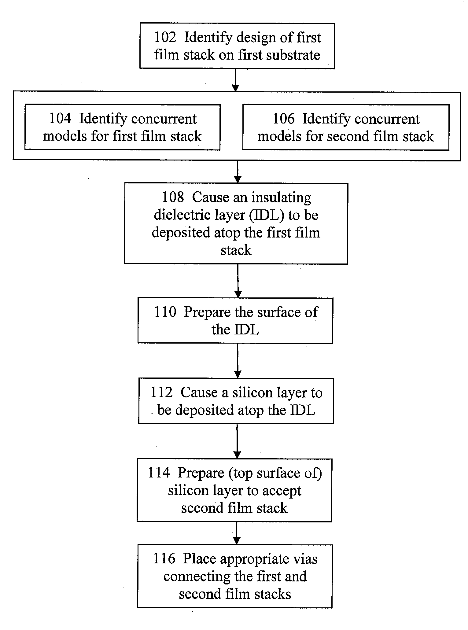
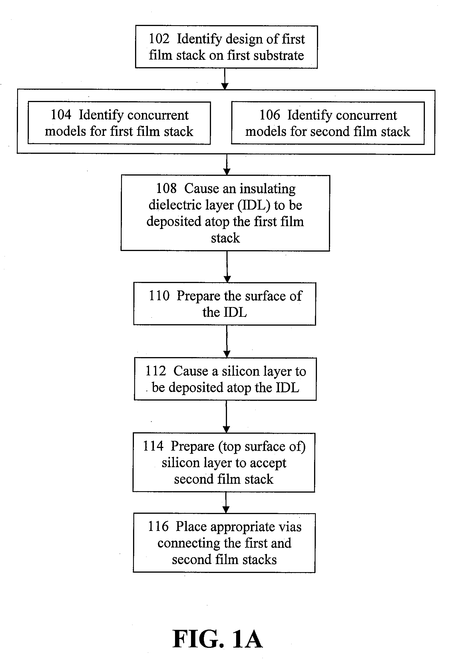
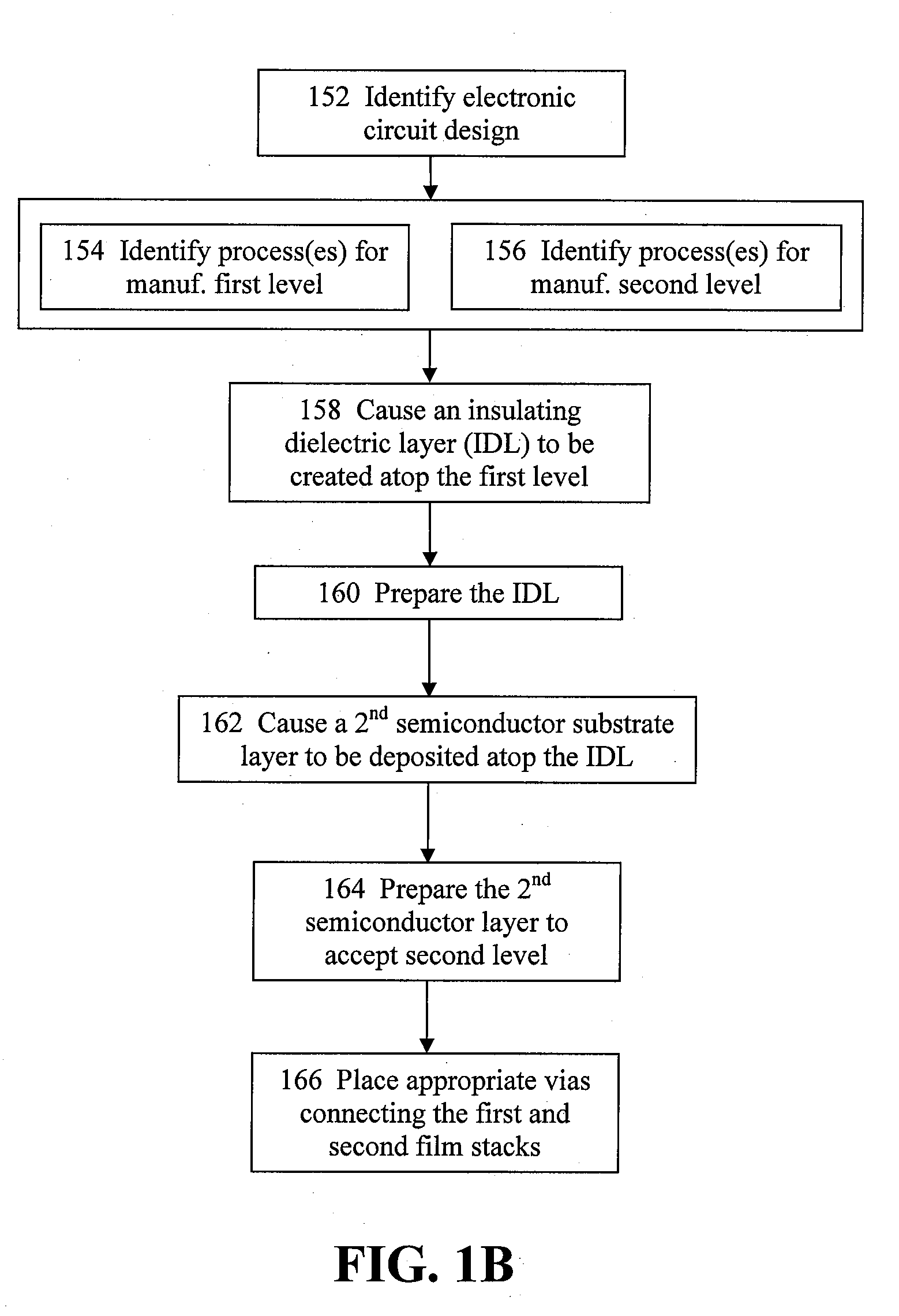
[0022]The present invention is directed to an improved method, system, and computer program product for preparing multiple levels of semiconductor substrates for three-dimensional integrated circuits (IC) integration. The method or the system of some embodiments of the invention analyzes the one or more insulating dielectric layers (IDL) separating the first and the second film stacks on separate substrates and then determines one or more characteristics which are required to enable the surface of the IDL to receive an additional layer of semiconductor substrate for further fabrication of the chips. The method or the system of some other embodiments of the present invention further employs the design model together with one or more concurrent models for the processes or techniques involved in the manufacturing of the integrated circuits to ensure that the IDL and the semiconductor substrate are sufficiently flat or smooth so the three-dimensional integrated circuits meet the reliabi...


PUM

PropertyMeasurementUnit
Contentaaaaaaaaaa
Stress optical coefficientaaaaaaaaaa
Surface roughnessaaaaaaaaaa

Abstract

Disclosed is an improved method, system, and computer program product for preparing multiple levels of semiconductor substrates for three-dimensional IC integration. Some embodiments utilize the process and design models to check and fabricate the insulating dielectric layer (IDL) separating the first and the second film stacks on separate substrates and then prepare the surface of the IDL to receive an additional layer of semiconductor substrate for further fabrication of the chips. Yet some other embodiments further employ the design and process models to ensure the IDL and the semiconductor substrate are sufficiently flat, or are otherwise satisfactory, so the three-dimensional integrated circuits meet the reliability, manufacturability, yield, or performance requirements. Yet some other embodiments further employ design and process models to place the vias connecting the multiple film stacks.

Description

CROSS-REFERENCE TO RELATED APPLICATION(S)[0001]This application claims the benefit of U.S. Provisional Application No. 60 / 878,000, filed on Dec. 29, 2006, which is hereby incorporated by reference in its entirety.BACKGROUND OF THE INVENTION[0002]The ever-growing demand for more functionality and higher performance has caused increased complexity in integrated circuit (IC) designs requiring more yet smaller transistors to be closely packed. As a result, the integrated circuit chip size has continually increased to accommodate the ever-increasing number of transistors. This continual demand for smaller features improves the performance of integrated circuits but also adversely impacts the interconnect performances. Smaller wire sizes and spacing and longer lines to traverse larger chip areas have increased the resistance, capacitance and, as a result, the R-C delay. Moreover, this interconnect delay becomes more significant and can no longer be ignored as the feature sizes continue to...

Claims


Application Information

Patent Timeline
IPC IPC(8): G06F17/50H01L21/66H01L21/64
CPCH01L2924/0002Y10T29/41H01L22/20H01L25/50H01L2924/00
Inventor SCHEFFER, LOUIS K.WHITE, DAVID
Owner CADENCE DESIGN SYST INC
Why Eureka
Try Eureka