Eureka AIR delivers breakthrough ideas for toughest innovation challenges, trusted by R&D personnel around the world.

Semiconductor device

a technology of semiconductor devices and resistors, applied in semiconductor devices, semiconductor/solid-state device details, electrical apparatus, etc., can solve the problems of increasing unwanted effects, power consumption, and inability to arrange a sufficient number of bypass capacitors and damping resistors, so as to reduce signal noise efficiently, high resistance, and high resistance

Inactive Publication Date: 2008-07-10
ELPIDA MEMORY INC +1
View PDF0 Cites 2 Cited by
  • Summary
  • Abstract
  • Description
  • Claims
  • Application Information

AI Technical Summary

Benefits of technology

[0014]In view of the problems as described above, it is an exemplary object of the present invention to provide a semiconductor device with a package substrate capable of suppressing the disturbance in the signal waveform and ensuring high signal quality.
[0016]The semiconductor device according to the present invention has a semiconductor chip mounted on the package substrate, and the package substrate wiring is composed of the predetermined or normal resistance material layer and the high resistance material layer which has the high resistance as compared with the predetermined resistance material layer. Most part of noise current of a high-speed operation signal transmitted through the wiring pattern of the package board or package substrate is composed of high frequency components. Signal noises such as overshoot, undershoot and ringing are generated by the increase of signal frequency. The use of a high resistance material layer on the face of the signal line facing the power supply line is effective to efficiently reduce the signal noises such as overshoot, undershoot, and ringing. Further, the high resistance material layer can be applied to between the signal line and the power supply plane in a reduced-size tape carrier package substrate to obtain a more enhanced noise reduction effect.

Problems solved by technology

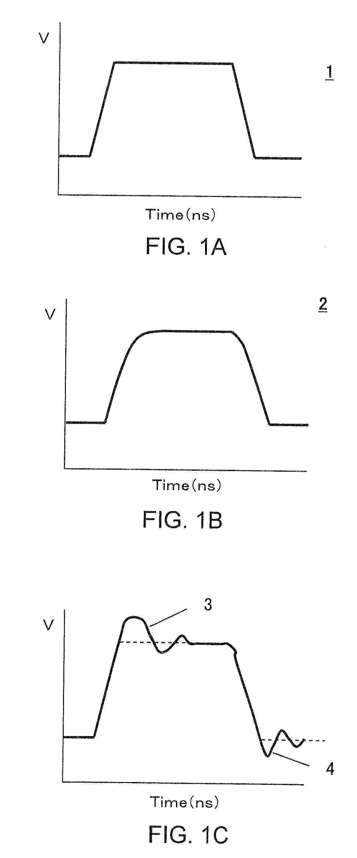
As described above, the recent increase of operational speed and reduction of power consumption of the semiconductor devices involves increase of unwanted effects exerted on signal transmission by noises generated by high-speed signals on a packaging board or package substrate.
However, the increased operational speed, decreased size, and increased density of the semiconductor devices have make it impossible to enlarge the area of power supply and ground lines, or to arrange a sufficient number of bypass capacitors and damping resistors.
This results in problems of occurrence of disturbance in the signal waveform, and deterioration of the signal quality.

Method used


Image

  • Semiconductor device
  • Semiconductor device
  • Semiconductor device

Examples


first exemplary embodiment

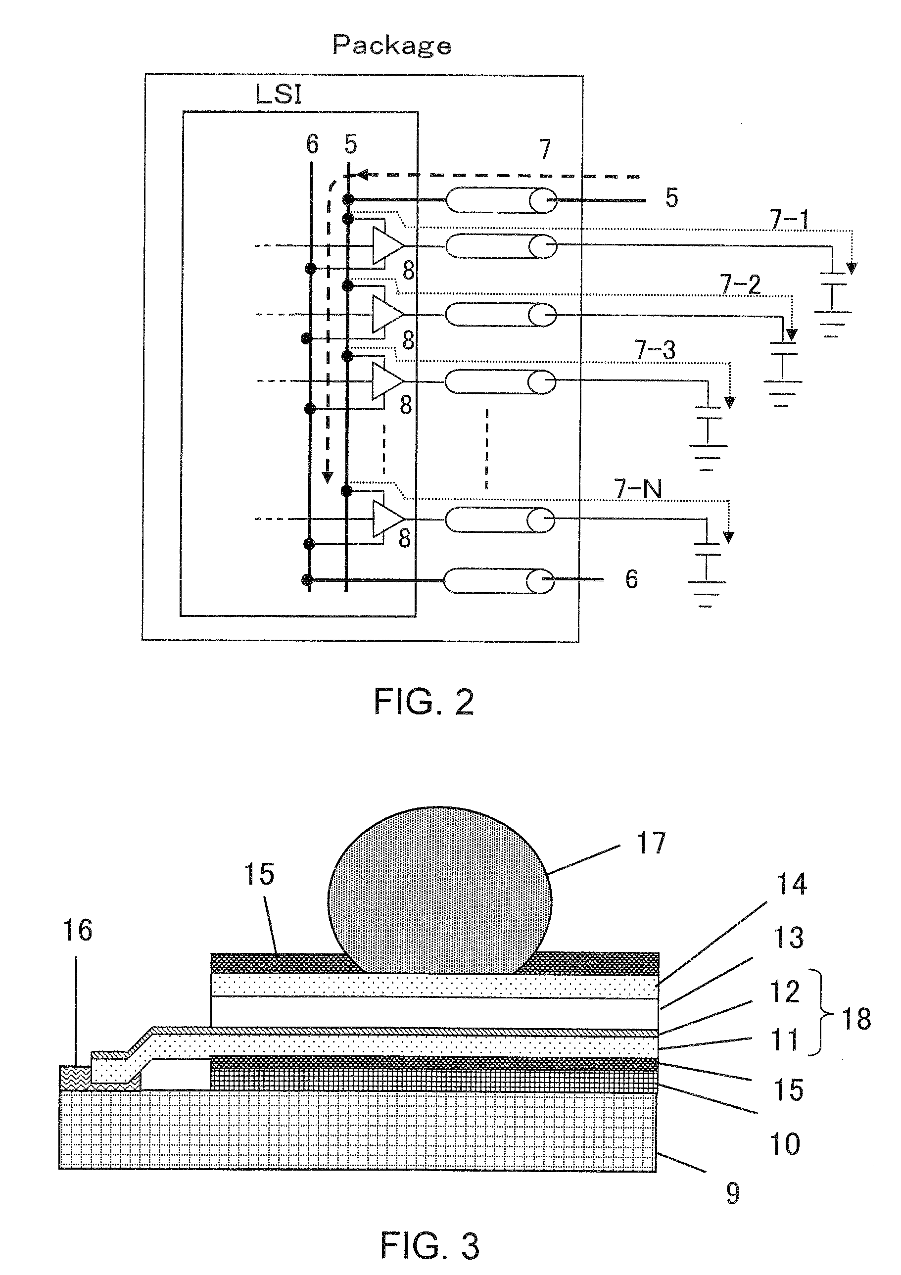
[0033]A semiconductor device according to first exemplary embodiment of the present invention will be described in detail with reference to FIGS. 3 to 8. FIG. 3 is a cross-sectional view showing a semiconductor device mounted on a two-layer wiring package substrate. FIGS. 4 to 6 are cross-sectional views or a plan view showing the respective manufacturing steps of the semiconductor device. FIG. 7 is a graph illustrating transmission loss between signal lines and a ground plane. FIG. 8 is a graph illustrating skin depth (depth at which current flows) depending on wiring materials of the package substrate.

[0034]FIG. 3 is a cross-sectional view of a semiconductor device according to the first exemplary embodiment of the present invention. The reference numeral 9 denotes a semiconductor chip, 10 denotes an elastomer, 11 denotes a predetermined resistance material layer. Herein, the predetermined resistance material layer may be, for example, a copper (Cu) layer which has a thickness of ...

second exemplary embodiment

[0045]A semiconductor device according to a second exemplary embodiment of the present invention will be described with reference to FIGS. 9 to 14. The second exemplary embodiment relates to a semiconductor device mounted on a single-layer wiring package substrate in which a high resistance material layer is provided only on a required side face or faces of each signal line. FIG. 9 is a cross-sectional view showing a package substrate in which a high resistance material layer is formed on the both side faces of a signal line. FIG. 10 is a cross-sectional view showing a package substrate in which a high resistance material layer is formed on the mutually facing side faces of adjacent differential signal lines. FIG. 11 is a cross-sectional view showing a package substrate in which differential signal lines are arranged between two ground lines, and a high resistance material layer is formed on the both side faces of the differential signal lines and on the side faces of the ground lin...

third exemplary embodiment

[0054]A semiconductor device according to a third exemplary embodiment of the present invention will be described with reference to FIG. 15. The third exemplary embodiment relates to a semiconductor device mounted on a double-layer wiring package substrate and provided with differential signal lines. FIG. 15 is a cross-sectional view of a package substrate in which the ground plane located between the differential signal lines is formed by a high resistance material layer. In the third exemplary embodiment as well, the predetermined or normal resistance material layer 11 is formed of a low resistance material such as Cu. that is commonly used low-resistance wiring material The high resistance material layer 12 is formed of a metal material having a higher resistance than Cu, for example of Omega-Ply RCM (trade name of Ni—P alloy manufactured by Omega Technology Corp.) or 42 alloy.

[0055]In FIG. 15, the reference numeral 21 denotes the normal resistance material layer (Cu) forming the...


PUM


Abstract

A semiconductor device is mounted on a package substrate which has a power supply line and a signal line formed of a normal or predetermined resistance material layer on a dielectric layer. A resistance material layer has a high resistance as compared with the normal resistance material layer and is additionally provided on the surface of the normal resistance material layer of the peripheral face of the signal line closest to the power supply line.

Description

[0001]This application is based upon and claims the benefits of priority from Japanese patent application No. 2006-345590, filed on Dec. 22, 2006, the disclosure of which is incorporated herein in its entirety by reference.BACKGROUND OF THE INVENTION[0002]1. Field of the Invention[0003]The present invention relates to a semiconductor device, and in particular, to a semiconductor device mounted on a package substrate capable of reducing signal noises.[0004]2. Description of the Related Art[0005]In recent years, the operational speed of semiconductor devices has been increased on one hand, while their power consumption has been reduced on the other hand. This leads to various problems which need not be addressed according to prior arts. The problems include those relating to signal integrity (SI) and power integrity (PI). The SI relates to a transmission waveform quality during signal transmission in a semiconductor device. The SI ensures digital signals having wide frequency componen...

Claims


Application Information

Patent Timeline
IPC IPC(8): H01L23/488
CPCH01L23/647H01L23/66H01L2223/6638H01L2924/19051H01L2924/0002H01L2924/3011H01L2924/00
Inventor KOSHIISHI, KAZUTAKAKATAGIRI, MITSUAKIISA, SATOSHIAKAHOSHI, HARUO
Owner ELPIDA MEMORY INC
Why Eureka
Eureka Blog
Learn More