Method for manufacturing semiconductor device

a semiconductor and manufacturing technology, applied in the direction of semiconductor devices, electrical devices, transistors, etc., can solve the problems of generating a lot of defects at the surface of the source/drain region, piping and spiking of nickel silicide, and current leakage, so as to improve the junction leakage phenomenon

Active Publication Date: 2008-07-10
UNITED MICROELECTRONICS CORP
View PDF5 Cites 5 Cited by
  • Summary
  • Abstract
  • Description
  • Claims
  • Application Information

AI Technical Summary

Benefits of technology

[0007]Accordingly, at least one objective of the present invention is to provide a method...

Problems solved by technology

However, nickel silicide possesses piping and spiking problems.
That is, after the nickel silicide is formed, the nickel silicide diffuses into the substrate and the channel regions and the diffusion of the nickel silicide leads to current leak...

Method used


Image

  • Method for manufacturing semiconductor device
  • Method for manufacturing semiconductor device
  • Method for manufacturing semiconductor device

Examples


Embodiment Construction

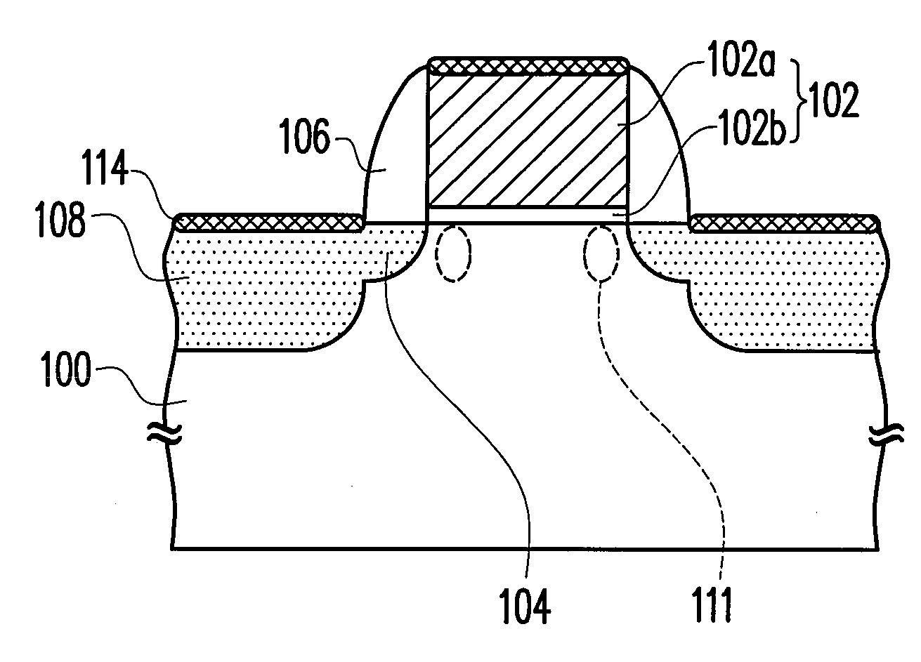
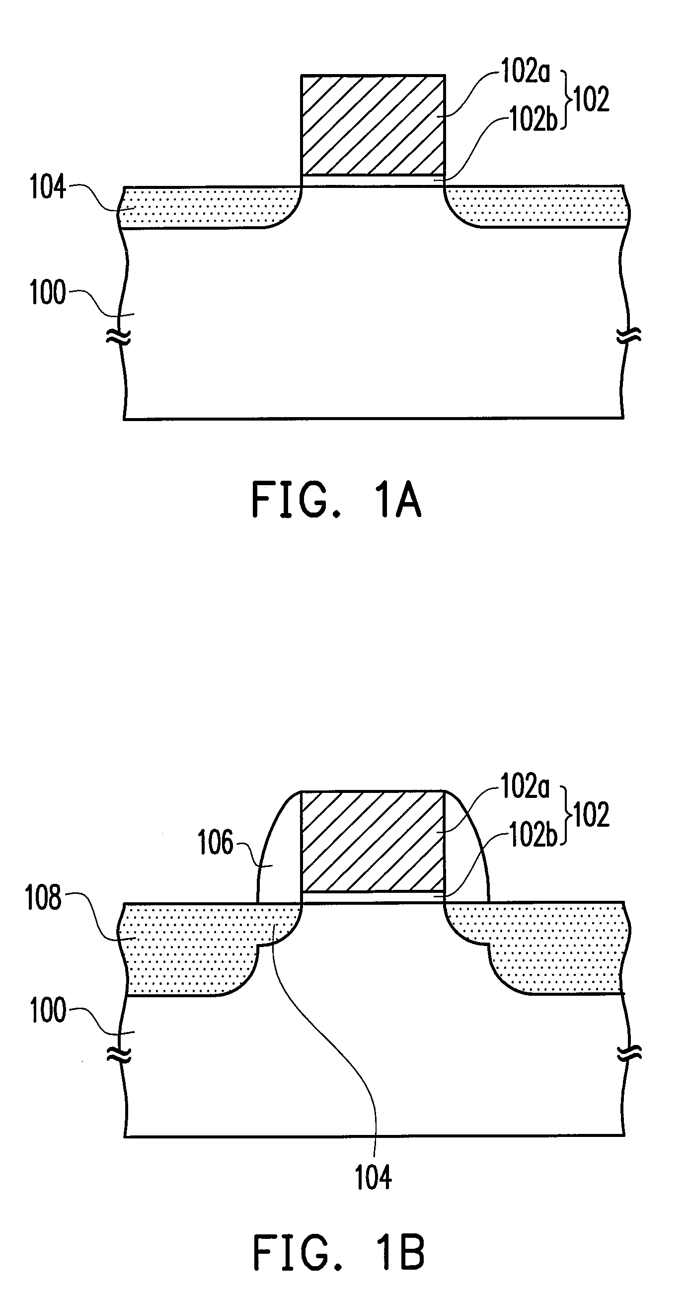
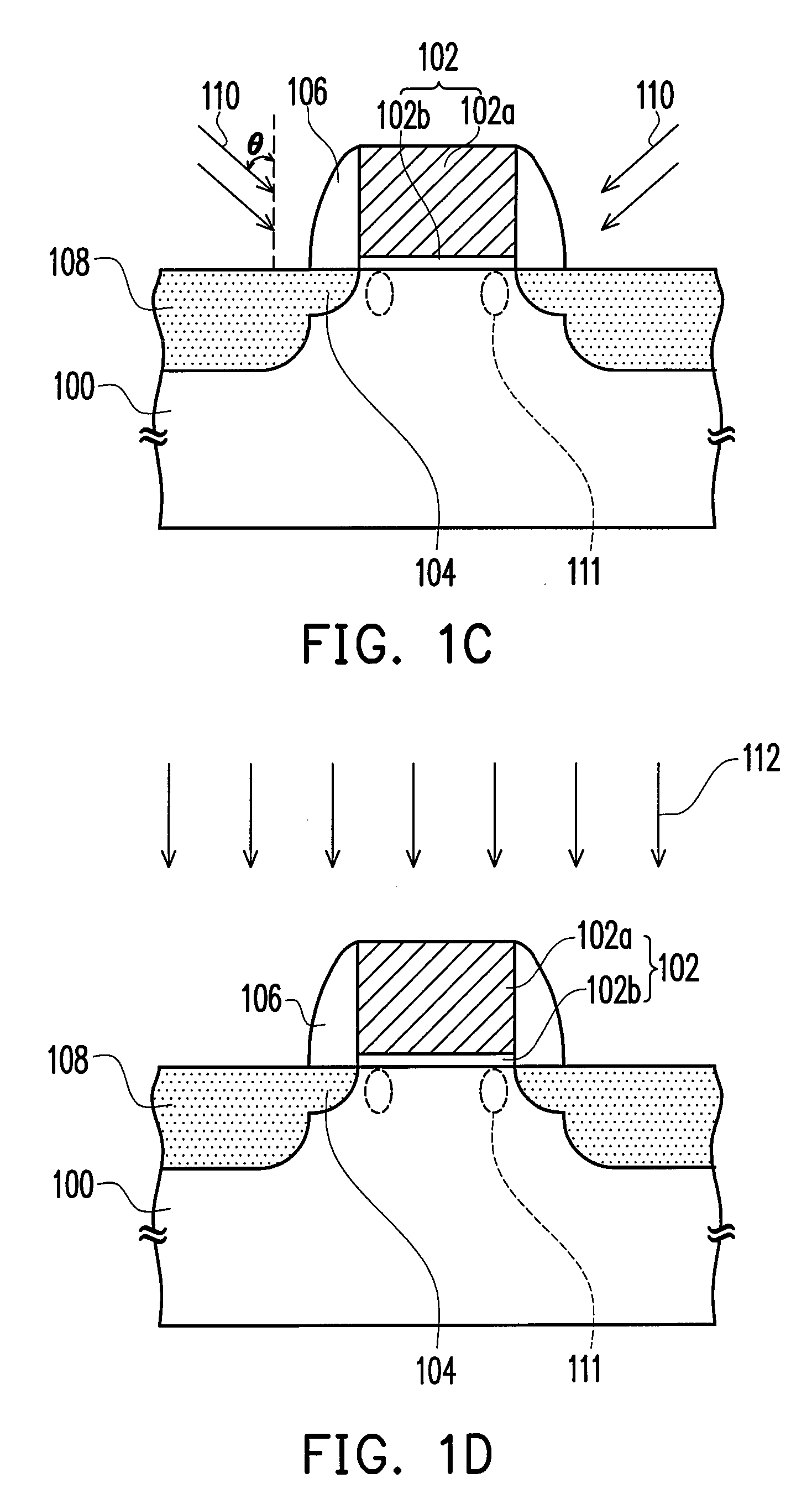
[0030]FIGS. 1A through 1E are cross-sectional views schematically illustrating a method for forming a semiconductor device according to a preferred embodiment of the invention. As shown in FIG. 1A, a gate structure 102 composed of a gate 102a and a gate dielectric layer 102b is formed on a substrate 100. The method for forming the gate structure 102 can be, for example, comprises steps of forming a dielectric material layer (not shown) and a gate material layer (not shown) over the substrate 100 sequentially and then patterning the gate material layer and the dielectric material layer into the gate structure 102 by using the photolithography process and the etching process. The dielectric material layer can be, for example but not limited to, made of silicon oxide, silicon nitride or silicon-oxy nitride. The gate material layer can be, for example, made of polysilicon or metal. Then, a source / drain extension region 104 is formed in the substrate 100 adjacent to the gate structure 10...


PUM


Abstract

The invention is directed to a method for manufacturing a semiconductor. The method comprises steps of providing a substrate having a gate structure formed thereon and forming a source/drain extension region in the substrate adjacent to the gate structure. A spacer is formed on the sidewall of the gate structure and a source/drain region is formed in the substrate adjacent to the spacer but away from the gate structure. A bevel carbon implantation process is performed to implant a plurality carbon atoms into the substrate and a metal silicide layer is formed on the gate structure and the source/drain region.

Description

BACKGROUND OF THE INVENTION[0001]1. Field of Invention[0002]The present invention relates to a method for manufacturing a semiconductor device. More particularly, the present invention relates to a method for manufacturing a semiconductor device capable of solving junction leakage problem.[0003]2. Description of Related Art[0004]With the decreasing of the size of the integrated circuit and the increasing of the integration of the integrated circuit, the line width, junction area and junction depth are decreased. To effectively increase the functionalities of the device and to decrease the resistance and signal transmission delay due to the resistance and the capacitance, the metal silicide is formed at the junction region to effectively decrease the contact resistance.[0005]In the well known self-aligned metal silicide manufacturing process, nickel silicide is formed at the surfaces of the gate, the spacer and the source / drain region of the metal-oxide semiconductor. However, nickel...

Claims


Application Information

Patent Timeline
IPC IPC(8): H01L21/04
CPCH01L21/26506H01L21/26586H01L29/7833H01L29/665H01L29/6659H01L29/1083
Inventor TING, SHYH-FANNHUANG, CHENG-TUNGJENG, LI-SHIANLEE, KUN-HSIENHUNG, WEN-HANCHENG, TZYY-MING
Owner UNITED MICROELECTRONICS CORP
Why Eureka
Try Eureka