Demodulator, Chip And Method For Digital Demodulating An Fsk Signal

a demodulator and signal technology, applied in the field of demodulators, chips and methods for digitally demodulating fsk signals, can solve the problems of large surface area occupied, excessive power dissipation in the tissue, and limited maximum carrier frequency of biomedical implants, etc., to achieve the effect of reducing the amount of surface area occupied

Inactive Publication Date: 2008-07-17
RGT UNIV OF MICHIGAN
View PDF57 Cites 6 Cited by
  • Summary
  • Abstract
  • Description
  • Claims
  • Application Information

AI Technical Summary

Benefits of technology

[0045]Further in carrying out the above object and other objects of the present invention, an FSK demodulator chip for an FSK data transmission system having a fully digital data transfer protocol is provided. The chip includes a substrate and a digital demodulator formed on the substrate for demodulating an FSK signal having a data rate from a carrier signal having a pair of carrier frequencies. The demodulator generates a serial data bit stream based on the FSK carrier signal and generates a synchronized constant frequency clock signal from the carrier frequencies based on the data transfer protocol for sampling the serial data bit stream. The demodulator is fully digital to minimize the amount of surface area occupied by the demodulator on the substrate.

Problems solved by technology

However, this is not the only application of data and power transfer via inductive coupling.
Achieving high power transfer efficiency, high data transfer bandwidth, and coupling insensitivity are some of the challenges that one would face in the design of such systems.
On the other hand, the maximum carrier frequency for biomedical implants is limited to a few tens of MHZ due to the coupled coils' self-resonant frequency, more power loss in the power transfer circuitry, and excessive power dissipation in the tissue, which increases as square of the carrier frequency [5].
This method, however, faces major limitations for high-bandwidth data transfer, because high-bandwidth ASK needs high order filters with sharp cut-off frequencies, whose large capacitors cannot be easily integrated in this low-frequency range of RF applications.
Specifically, the common FSK demodulation techniques need some kind of analog filtering down the signal path, which consume even more chip area due to the above-noted low-end RF application.
Analog circuits are more susceptible to process and temperature variations and their design becomes more challenging with the trend towards smaller feature size and lower power supply voltage.

Method used


Image

  • Demodulator, Chip And Method For Digital Demodulating An Fsk Signal
  • Demodulator, Chip And Method For Digital Demodulating An Fsk Signal
  • Demodulator, Chip And Method For Digital Demodulating An Fsk Signal

Examples


Embodiment Construction

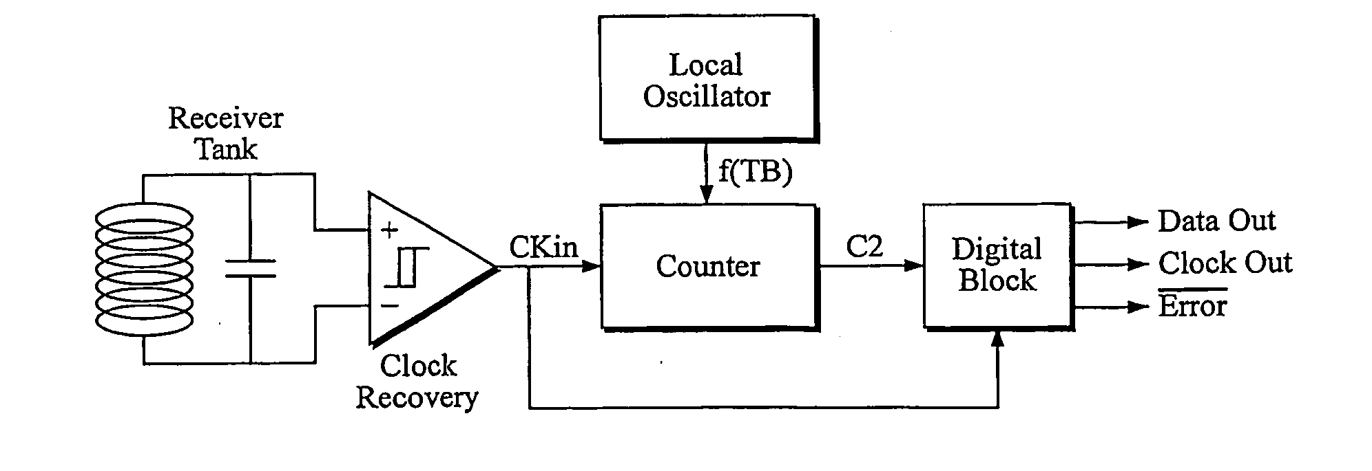
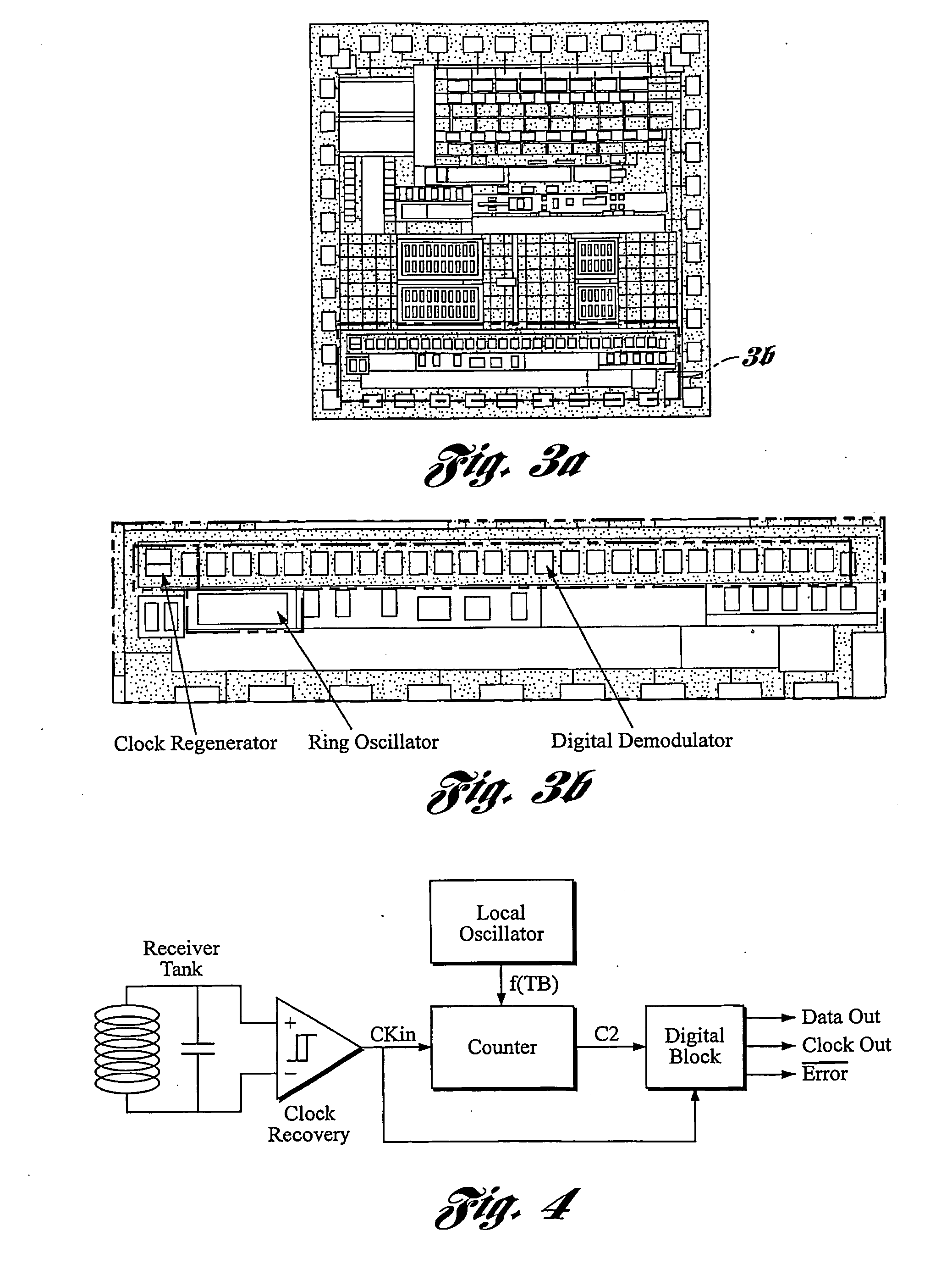
[0068]In general, an improved demodulator, chip and method for digitally demodulating an FSK signal is described herein. In this digital approach, the received FSK carrier is dealt with as a base-band signal. The data detection technique used here for the FSK demodulation is based on digitally measuring the period of each received carrier cycle. If the period is higher than a certain value, a digital “1” bit is detected and otherwise a digital “0” is received.

[0069]As previously described, a simple method for time measurement in an analog circuit is charging a capacitor with a constant current source and monitoring its voltage [9, 10]. However, in a digital circuit one can count a constant frequency clock time-base (fTB) at a rate several times higher than the carrier frequency. Most often this internal clock, which does not need to be synchronized with the carrier, is already available in the system for running other digital circuits or the processor. An n-bit counter runs while th...


PUM


Abstract

A demodulator, chip and method for digitally demodulating an FSK signal utilizing a digital data transfer protocol and a digital demodulator circuit have been developed. The data-rate approaches the carrier-frequency. The one application for this technique is in the magnetically powered wireless systems such as biomedical implants and radio frequency identification (RFID) tags with high data rates above 1 Mbps. The demodulator circuit extracts the serial data bit-stream and a constant-frequency clock from an FSK carrier signal in the 1˜20 MHZ range, which can power the wireless system as well. The digital demodulator circuit is implemented entirely with digital circuitry and is called a digital-FSK (DFSK) demodulator.

Description

CROSS-REFERENCE TO RELATED APPLICATION[0001]This application claims the benefit of U.S. provisional application Ser. No. 60 / 538,178, filed Jan. 22, 2004 and entitled “Frequency Shift Keying Demodulation Methods for Wireless Biomedical Implants.”STATEMENT REGARDING FEDERALLY SPONSORED RESEARCH OR DEVELOPMENT[0002]This invention was made with Government support from The National Institute of Health under Contract No. NIH-NINDS-N01-NS-9-2304. The Government has certain rights in the invention.BACKGROUND OF THE INVENTION[0003]1. Field of the Invention[0004]This invention relates to demodulators, chips and methods for digitally demodulating FSK signals.[0005]2. Background Art[0006]The following references may be referenced herein:[0007][1] P. R. Troyk, I. E. Brown, W. H. Moore and G. E. Loeb, “Development of BION Technology for Functional Electrical Stimulation: Bidirectional Telemetry,” 23rd IEEE-EMBS Conference Proceedings, Vol. 2, pp. 1317-1320, 2001.[0008][2] D. G. Galbraith, M. Soma...

Claims


Application Information

Patent Timeline
Patent Type & Authority Applications(United States)
IPC IPC(8): H03D3/00
CPCH03D3/006
Inventor GHOVANLOO, MAYSAMNAJAFI, KHALIL
Owner RGT UNIV OF MICHIGAN
Why Eureka
Try Eureka