Solid-state imaging device and camera using the same

a technology of solid-state imaging and camera, which is applied in the field can solve the problems of color-tone changes, such as the color-fading of pigments, deterioration of color separation functions, and increase the manufacturing cost of solid-state imaging devices, and achieves the effects of suppressing sensitivity decline, high wavelength sensitivity (color resolution), and high picture quality

Inactive Publication Date: 2008-07-17
PANASONIC CORP
View PDF7 Cites 103 Cited by
  • Summary
  • Abstract
  • Description
  • Claims
  • Application Information

AI Technical Summary

Benefits of technology

[0011]Meanwhile, in the unit pixel as shown in FIG. 2, the film thickness of the color filter is as large as 1 μm or more in order to realize high wavelength sensitivity (color resolution). Therefore, along with the scaling down of pixels in recent years, the light transmitted through the microlens invades an adjacent pixel due to the large thickness of the color filter. For example, color mixing occurs in which the color of G or B is mixed into the color of R, causing deterioration in the color separation function. As a result, a color filter which can suppress sensitivity decline and color unevenness resulting from the scaling down of pixels is anticipated. In other words, the color filter which can realize a solid-state imaging device of higher picture quality is anticipated.
[0012]In addition, in the forming of on-chip color filters, forming processes using photo masks are required for each of the colors. Therefore, in order to form three types of color filters R, G, and B, for example, three types of photo masks are needed. Therefore, such conventional on-chip color filters become a factor for raising manufacturing costs for the solid-state imaging device. As a result, an on-chip color filter which can reduce costs by shortening the manufacturing time and improve the yield is desired.

Problems solved by technology

For example, color mixing occurs in which the color of G or B is mixed into the color of R, causing deterioration in the color separation function.
Therefore, such conventional on-chip color filters become a factor for raising manufacturing costs for the solid-state imaging device.
Furthermore, since conventional color filters are made of pigments, color-tone changes, such as the color-fading of the pigments, occur over time under high temperature conditions, such as in the open air.
Therefore, conventional color filters have great problems in their reliability.

Method used


Image

  • Solid-state imaging device and camera using the same
  • Solid-state imaging device and camera using the same
  • Solid-state imaging device and camera using the same

Examples


first embodiment

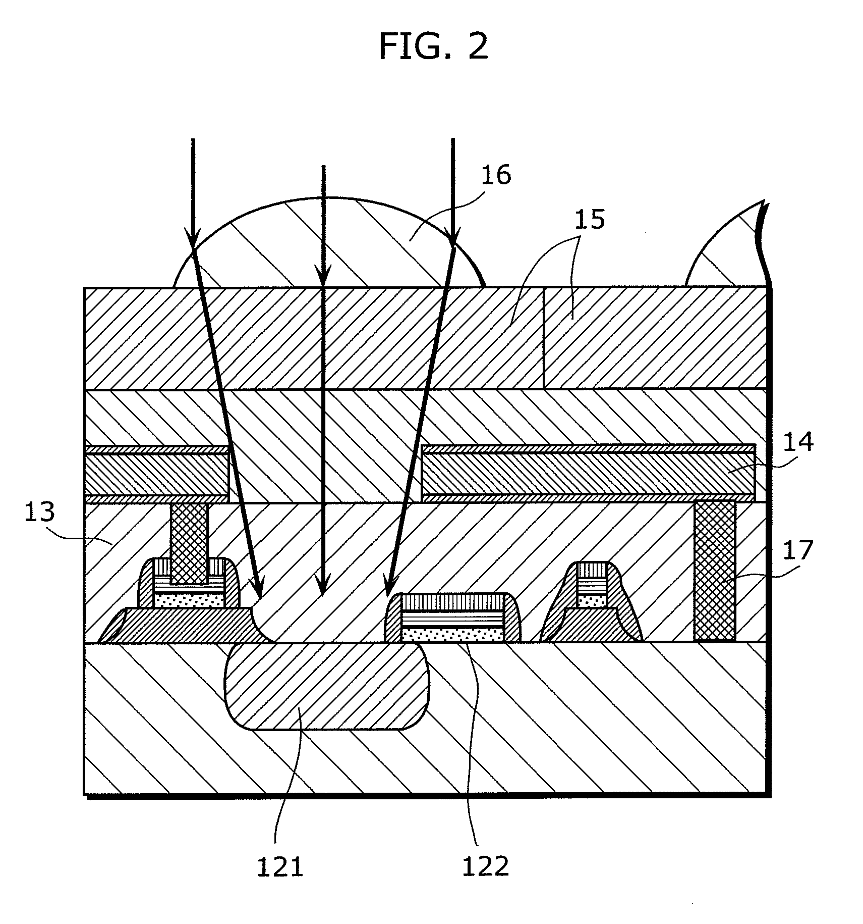
[0073]In the solid-state imaging device according to the present embodiment, a metal optical filter, which allows light of a desired wavelength to be transmitted, is formed above a photodiode (light-receiving element), such as a photodiode, which converts received light into an electric signal, and with an insulating film sandwiched in between the metal optical filter and the photodiode. This metal optical filter is an optical filter made of a metal thin film, and in the metal optical filter, plural apertures are periodically provided in a two-dimensional state. Note that the plural apertures may also be arrayed in a one-dimensional state.

[0074]Hereinafter, the behavior of the light with respect to the apertures provided in the metal thin film and periodically arrayed in a two-dimensional state shall be described focusing on a single aperture, and then shall be described focusing on plural apertures that are periodically arrayed. Note that the apertures in the metal thin film are re...

second embodiment

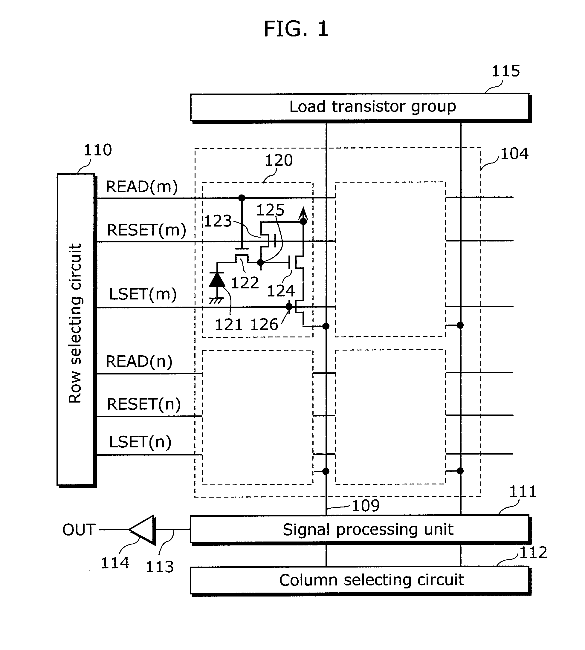
[0088]The solid-state imaging device according to the present embodiment is different from the solid-state imaging device in the first embodiment in that photodiodes are arrayed in a two-dimensional state and that a metal optical filter is provided in a two-dimensional state corresponding to each of the photodiodes. Specifically, the solid-state imaging device according to this embodiment is different in that a photodiode is provided with respect to each pixel which is the smallest unit constituting an image that is taken, that a metal optical filter is formed above each photodiode, and that an aperture is provided in the upper part of the pixel on a pixel-to-pixel basis.

[0089]By providing a metal optical filter above a photodiode for each pixel, it is possible to design spectral properties for the metal optical filter so that a different color signal can be obtained with each pixel. In a solid-state imaging device, such as a CCD solid-state imaging device and a MOS solid-state imag...

third embodiment

[0091]The solid-state imaging device according to the third embodiment of the present invention is different from the solid-state imaging device in the first or the second embodiment in that apertures are cylinder-shaped.

[0092]As described earlier, the waveguide cutoff wavelength λcutoff changes according to the shape of its aperture. In addition, the intra-waveguide wavelength λg differs in accordance with the polarization of light which enters through the aperture. Therefore, it is possible to prevent the cutoff wavelength λcutoff or the intra-waveguide wavelength λg from being dependent on the polarization direction by forming the apertures in a cylindrical or a column-like shape and making the cross-sectional structure of the apertures into a circular shape. As a result, an optical filter which has an equivalent filter function for every polarization direction can be realized.

[0093]In addition, the solid-state imaging device according to this embodiment is different from the sol...


PUM


Abstract

The object of the present invention is to provide a solid-state imaging device equipped with a color filter which is highly durable, inexpensive to manufacture, and adaptable to the scaling down of pixels, and a camera using the solid-state imaging device. The solid-state imaging device includes a photodiode, and a metal optical filter formed above the photodiode, which allows light of a desired wavelength to be transmitted. The metal optical filter is made of a metal thin film in which plural cylinder-shaped apertures are periodically arrayed. The size of each of the apertures is smaller than the desired wavelength, and an inter-aperture distance between a predetermined aperture and an aperture adjacent to the predetermined aperture is shorter than the desired wavelength.

Description

BACKGROUND OF THE INVENTION[0001](1) Field of the Invention[0002]The present invention relates to a solid-state imaging device equipped with a filter which cuts off light of an unnecessary wavelength within a wavelength band in which a photodiode is sensitive. The present invention also relates to a method for manufacturing the solid-state imaging device and a digital camera using the solid-state imaging device, or the like.[0003](2) Description of the Related Art[0004]Conventionally, a multiple-chip system and a single-chip system have been known as color separation techniques for the solid-state imaging device. In the multiple-chip system, color separation is performed on an image using a color separation prism, and the color-separated image is converted into an electric signal by three or four solid-state imaging devices, and color signals are obtained. On the other hand, in the single-chip system, color separation is performed on an image using on-chip color filters in three or ...

Claims


Application Information

Patent Timeline
Patent Type & Authority Applications(United States)
IPC IPC(8): H04N5/335G02B5/20H01L27/14H04N5/369
CPCH01L27/14621H01L27/14625H01L27/14685H01L27/14645H01L27/14632
Inventor YOSHIDA, SHINJI
Owner PANASONIC CORP
Why Eureka
Try Eureka