Plasma processing apparatus

a processing apparatus and plasma technology, applied in the direction of electrical apparatus, process and machine control, instruments, etc., can solve the problems of not being able to change the distribution of the electrode temperature at a high speed, and not being able to make the temperature (distribution) of the sample surface follow a desired value. , to achieve the effect of improving the efficiency of processing samples

US20080170969A1Inactive Publication Date: 2008-07-17HITACHI HIGH-TECH CORP
6 Cites 43 Cited by

Patent Information

Authority / Receiving Office
US · United States
Patent Type
Applications(United States)
Current Assignee / Owner
Publication Date
2008-07-17
Estimated Expiration
Not applicable · inactive patent

Smart Images

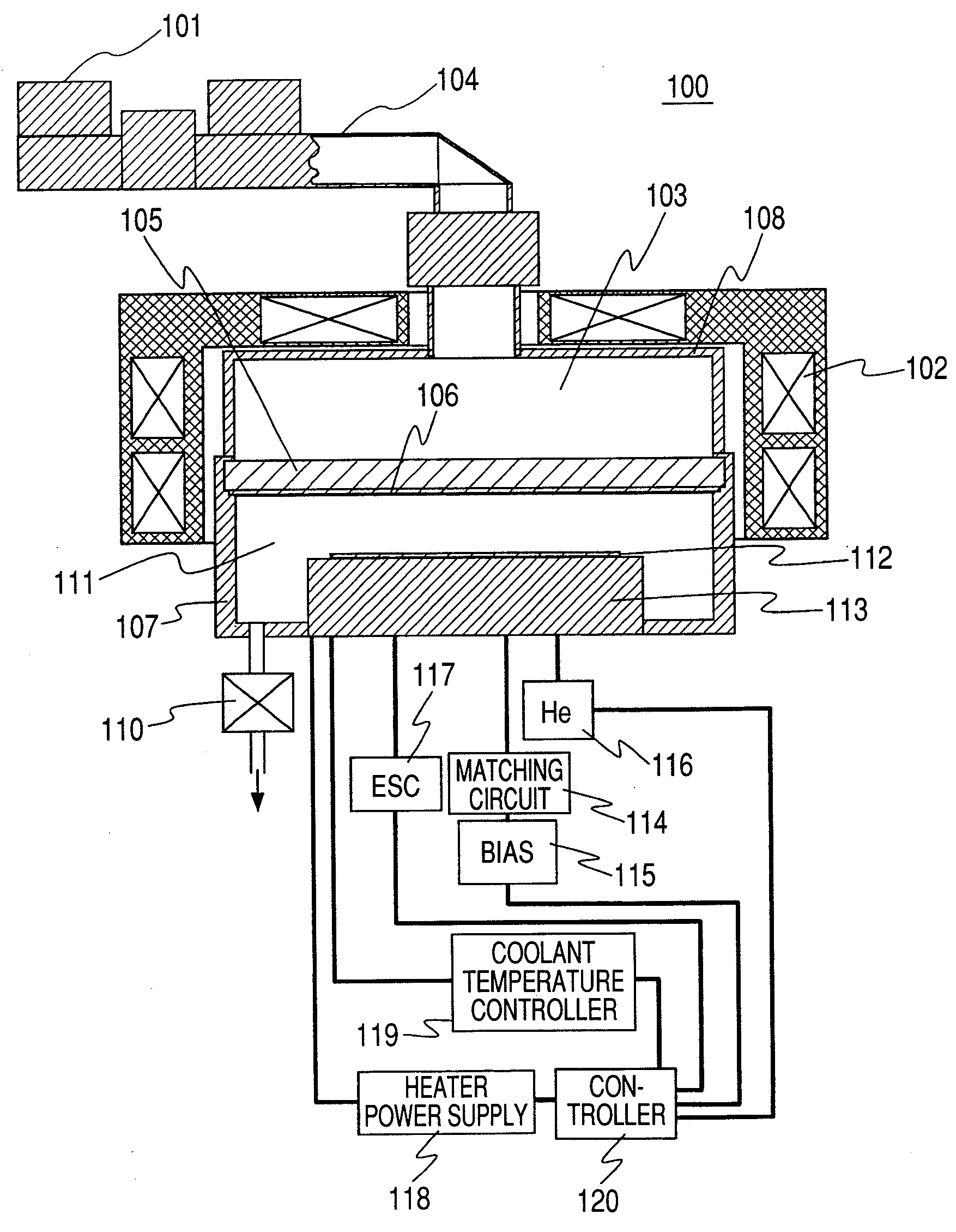
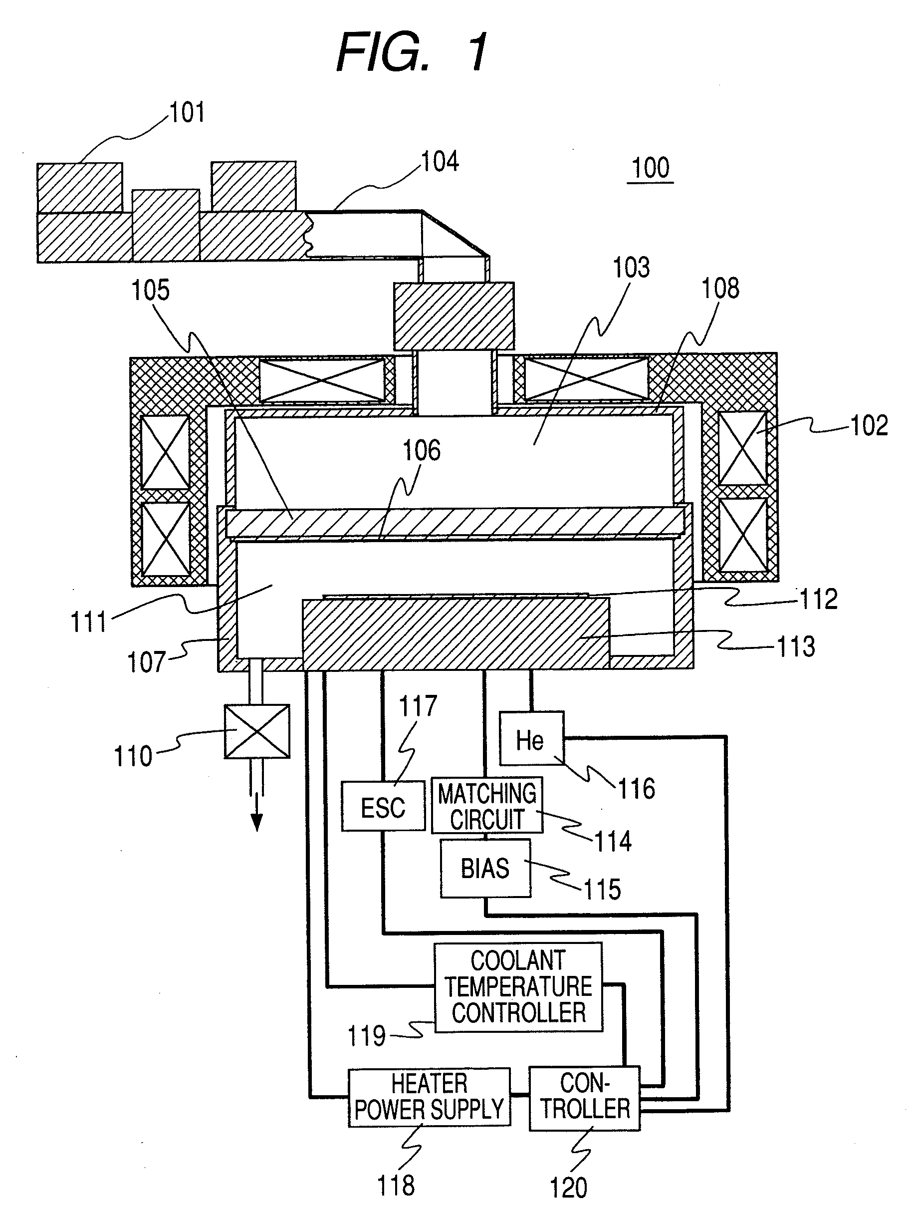
  • Figure 1
    Figure 1
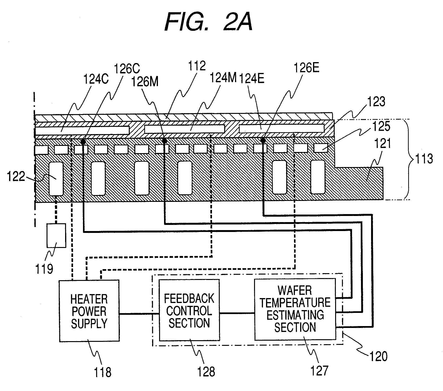
  • Figure 2
    Figure 2
  • Figure 3
    Figure 3
Patent Text Reader

Abstract

It is possible to provide a plasma etching apparatus that controls the temperature of a sample at a higher speed and with more accuracy to improve the efficiency of processing the sample. A plasma processing apparatus includes a processing chamber to be depressurized and exhausted, a sample placement electrode provided in the processing chamber and having a sample placement surface on which a substrate to be processed is placed, an electromagnetic generation device to generate plasma in the processing chamber, a supply system that supplies processing gas to the processing chamber, a vacuum exhaust system that exhausts inside the processing chamber, a heater layer and a base temperature monitor that are disposed on the sample placement electrode, a wafer temperature estimating unit that estimates a wafer temperature from the base temperature monitor and plasma forming power supply, and a controller that regulates the heater corresponding to output from the temperature estimating unit.
Need to check novelty before this filing date? Find Prior Art

Description

CLAIM OF PRIORITY

[0001] The present application claims priority from Japanese application JP 2007-8241 filed on Jan. 17, 2007, the content of which is hereby incorporated by reference into this application.FIELD OF THE INVENTION

[0002] The present invention relates to plasma processing apparatuses, such as a plasma etching apparatus provided with a sample stage suitably used to process a substrate-shaped sample, which is a processing target, or a plasma CVD apparatus suited to performing ion implantation or sputtering.BACKGROUND OF THE INVENTION

[0003] In plasma processing apparatuses, such as etching apparatuses and CVD apparatuses, etching has been conducted by supplying micro waves or an electric field in a high frequency range into a vacuum container; forming plasma in a processing chamber inside the vacuum container in whose lower part an electrode that is a sample stage on which a sample to be processed, such as a semiconductor wafer, is to be placed is previously disposed; and app...

Examples

embodiment

[0034]The embodiment according to the invention will be described referring to FIGS. 1 to 4.

[0035]FIG. 1 is a longitudinal sectional view schematically showing composition of a plasma etching apparatus according to this embodiment. As shown in FIG. 1, a plasma etching apparatus includes an approximately cylindrical processing chamber 111 disposed in a vacuum container 107 and depressurized, and a microwave source 101, formed of a magnetron, and a waveguide 104 that are both disposed above the processing chamber 111. The lower end of the waveguide 104 is coupled to a resonation container 108 disposed in an upper part of the vacuum container 107 so that the inside of the waveguide 104 and the resonation chamber 103 inside the resonation container 108 communicate with each other. Microwaves propagated from the microwave source 101 through the waveguide 104 are introduced into the resonation chamber 103 and resonated in a predetermined mode. Disposed between the resonation chamber 103 a...