Memory card and manufacturing method of the same

a memory card and manufacturing method technology, applied in the field of memory cards, can solve the problems of limiting the number of semiconductor chips and complicat and achieve the effect of simplifying the memory card manufacturing process

Inactive Publication Date: 2008-07-24
RENESAS ELECTRONICS CORP
View PDF6 Cites 41 Cited by
  • Summary
  • Abstract
  • Description
  • Claims
  • Application Information

AI Technical Summary

Benefits of technology

[0019]A memory card manufactur

Problems solved by technology

This limits the number of semiconductor chips when they are mounted on the w

Method used


Image

  • Memory card and manufacturing method of the same
  • Memory card and manufacturing method of the same
  • Memory card and manufacturing method of the same

Examples


first embodiment

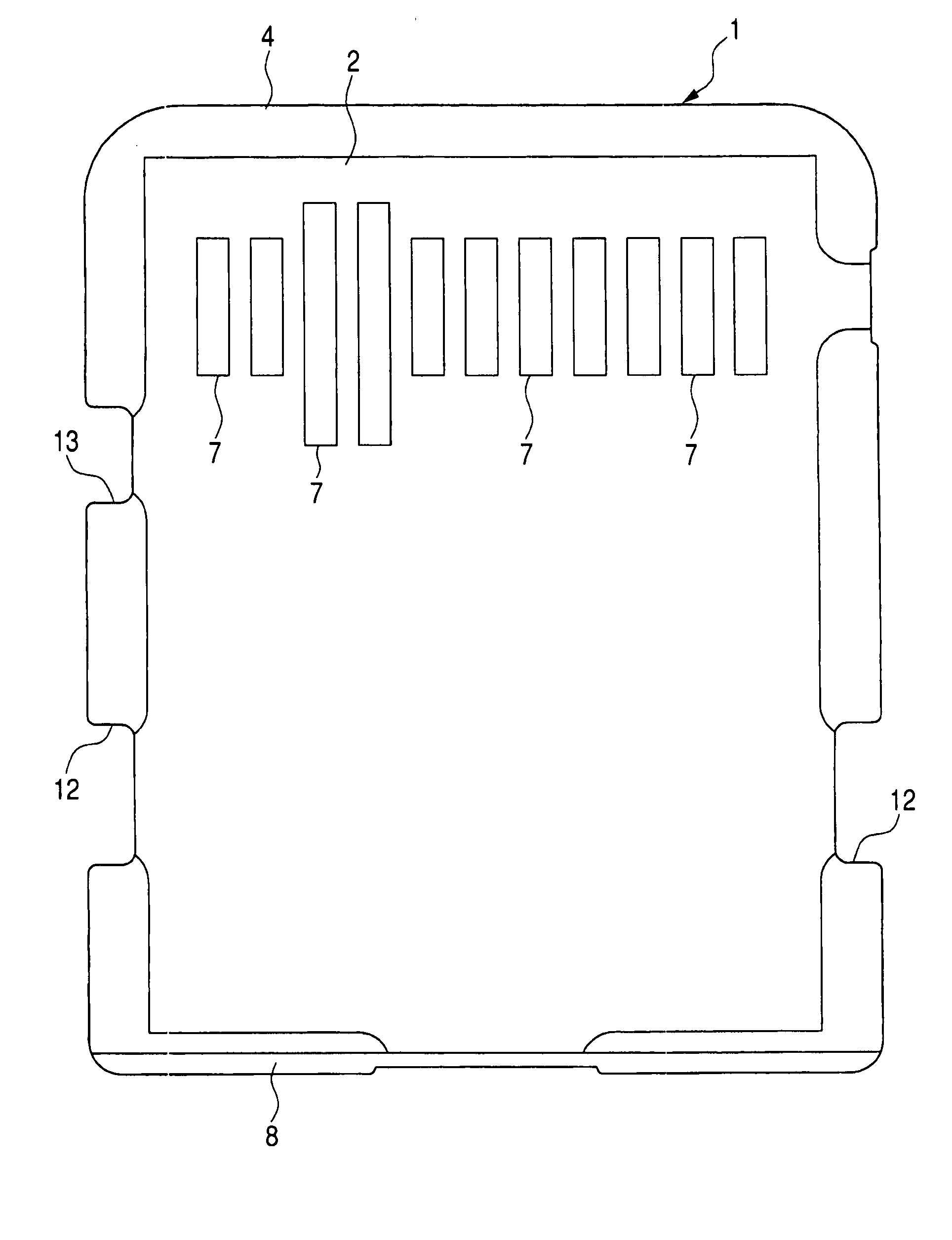
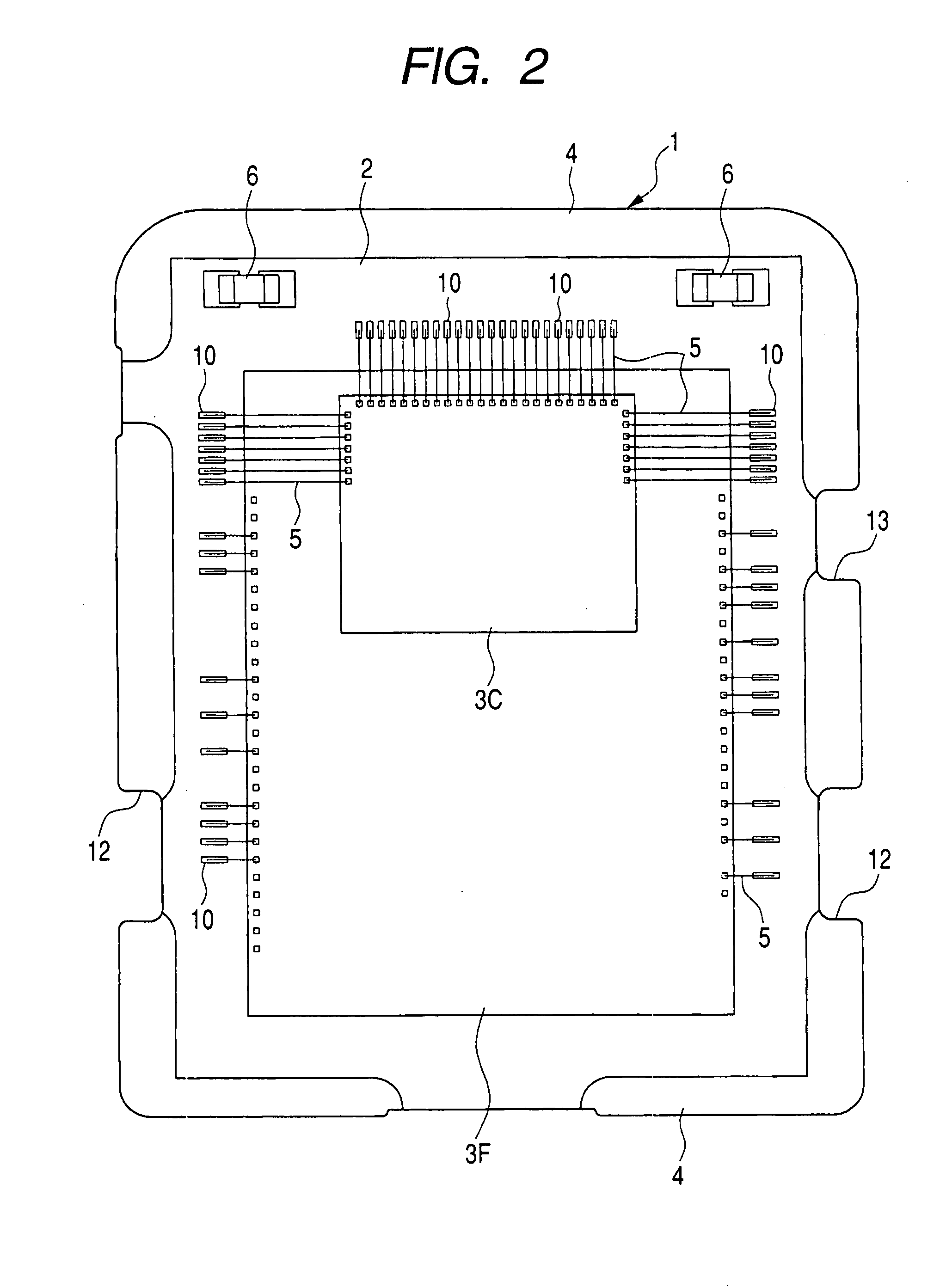
[0042]FIG. 1 is a plan view showing an external view (first surface) of a memory card according to the embodiment. FIG. 2 is a plan view showing an internal structure of the memory card according to the embodiment. FIG. 3 is a plan view showing an external view (back surface) of the memory card according to the embodiment. FIG. 4 is a cross sectional view taken along line A-A of FIG. 1. FIG. 5 is a cross sectional view taken along line B-B of FIG. 1.

[0043]A memory card 1 according to the embodiment is attached to a card slot of a mobile phone and is designed in compliance with the Memory Stick Micro standard. That is, the memory card 1 has an outside dimension of 16×12.5 mm and is 1.2 mm thick (1.6 mm thick only at a part forming a convex portion)

[0044]The memory card 1 includes: a wiring board 2 mainly composed of a glass epoxy resin; multiple semiconductor chips (3C and 3F) mounted on a main surface (first surface) of the memory card 1; and a mold resin 4 for encapsulating the wir...

second embodiment

[0085]FIG. 20 is an example of layering the semiconductor chips 3F by shifting them over the main surface of the wiring board 2 so as not to cover a wire bonding region of the semiconductor chip 3F for a lower layer with the semiconductor chip 3F for an upper layer. This example eliminates the need to provide the dummy chip (space chip 9) between the semiconductor chips 3F for the upper and lower layers as described in the above-mentioned embodiment. Much more semiconductor chips 3F can be mounted.

[0086]The semiconductor chip 3C constituting the interface controller may be layered over the semiconductor chip 3F or may be mounted directly on the main surface of the wiring board 2. Obviously, the memory chip (semiconductor chip 3F) may contain not only semiconductor memory other than the flash memory but also a mixture of the flash memory and the other semiconductor memory.

[0087]The memory card manufacturing method according to the invention can make the size of the mold resin 4 large...

third embodiment

[0091]The first embodiment has described the example of using the semiconductor chip 3F having a smaller planar dimension than that of the wiring board 2. As shown in FIG. 21, it is possible to use the semiconductor chip 3F having the same planar dimension as that of the wiring board 2. The prior art does not form a mold resin over a region that exceeds the planar dimension of the wiring board. When a semiconductor chip has the same planar dimension as that of the wiring board, an edge of the semiconductor chip is not covered with the mold resin and is exposed. Accordingly, the prior art cannot adopt the construction according to the embodiment.

[0092]As mentioned in the first embodiment, the third embodiment can permit a region for forming the mold resin 4 to have a larger planar dimension than that of the wiring board 2. Even when the semiconductor chip 3F to be used has the same planar dimension as that of the wiring board 2, the mold resin 4 can cover edges of the semiconductor c...


PUM


Abstract

There is a need to provide a large capacity memory card for a portable communication device. A memory card 1 includes: a wiring board 2 mainly composed of a glass epoxy resin; multiple semiconductor chips (3C and 3F) mounted on a main surface of the memory card 1; and a mold resin 4 for encapsulating the wiring board 2 and the semiconductor chips (3C and 3F). The mold resin 4 is made of a thermosetting epoxy resin containing quartz filler. A back surface of the wiring board 2 is not covered with the mold resin 4 and is exposed to a back surface of the memory card 1. The back surface of the wiring board 2 is used to form multiple external connection terminals 7 electrically connected to the semiconductor chips (3C and 3F) . When the memory card 1 is attached to a card slot of a mobile phone, the external connection terminals 7 contact with a connector terminal contained in the card slot. This makes it possible to exchange signals between the memory card 1 and the mobile phone or to supply the power.

Description

BACKGROUND OF THE INVENTION[0001]The present invention relates to a memory card and its manufacturing technology. More specifically, the invention relates to a technology effectively applicable to a small thin memory card attached to a card slot of a portable communication device.[0002]A recent mobile phone is provided with not only a telephone function but also the other functions such as network connection, e-mail transmission, image capturing, and navigation. Most recently, there is a trend of providing the security function such as a contactless IC card.[0003]The advent of multifunctional mobile phones necessitates development of various cards attached to a memory card slot of a mobile phone so as to provide smaller, thinner, and more multifunctional cards.[0004]Japanese patent laid-open No. 2005-339496 (Patent Document 1) discloses a small, large-capacity memory card (multifunction memory card) having the memory and security functions for mobile phones.[0005]The memory card dis...

Claims


Application Information

Patent Timeline
IPC IPC(8): H01L23/48H01L21/56
CPCH01L21/566H01L23/3121H01L2924/014H01L2924/01006H01L24/48H05K2203/1316H05K2201/10159H05K2201/09145H01L24/45H01L24/49H01L25/0657H01L25/18H01L2224/45144H01L2224/48091H01L2224/48227H01L2224/49175H01L2225/0651H01L2225/06562H01L2924/01004H01L2924/01005H01L2924/01033H01L2924/01079H01L2924/01082H01L2924/14H01L2924/19041H05K1/117H05K3/0052H05K3/284H01L2924/00014H01L2924/00H01L2924/181H01L2924/00012
Inventor KURATOMI, BUNSHISHIMIZU, FUKUMISUGIYAMA, MICHIAKIFUJISHIMA, ATSUSHIWADA, TAMAKI
Owner RENESAS ELECTRONICS CORP
Why Eureka
Try Eureka