Casting method of silicon ingot and cutting method of the same

a technology of silicon ingots and cutting methods, which is applied in the direction of polycrystalline material growth, crystal growth process, crystal growth process, etc., can solve the problems of generating cracks, accumulating stresses, and taking a long time to achieve cracks, and enhancing manufacturing efficiency, the effect of increasing the amount of casting per unit tim

Inactive Publication Date: 2008-07-31
SUMCO CORP
View PDF19 Cites 38 Cited by
  • Summary
  • Abstract
  • Description
  • Claims
  • Application Information

AI Technical Summary

Benefits of technology

[0022]The electromagnetic casting method excels the casting method in the following points that: the above molten silicon does not come into contact with the crucible; it is not necessary to use the high-purity material for the crucible; and the manufacturing efficiency thereof is high. However, the electromagnetic casting method is demanded to further enhance the manufacturing efficiency of the silicon ingot and the production yield in order to further reduce the manufacturing cost of the solar battery.
[0023]For dramatically enhancing the manufacturing efficiency of the silicon ingot, it is conceivable to enhance the cooling capacity of the water-cooling copper crucible and increase the casting speed by accelerating the solidification. However, as to the acceleration of solidification by enhancing the cooling capacity, there are concerns about the accumulation of stresses due to a great temperature gradient generated in a cast ingot, and the generation of cracks accompanied therewith.
[0024]It is also conceivable to enhance the manufacturing efficiency by analogously increasing the sectional area of the ingot and increasing the amount of casting per unit time. However, if this method is used, it will increase the distance from the center of the ingot to the side thereof, therefore, it takes a long time until the molten silicon completely solidifies, which increases the depth of an interface of solid and liquid phases.

Problems solved by technology

However, as to the acceleration of solidification by enhancing the cooling capacity, there are concerns about the accumulation of stresses due to a great temperature gradient generated in a cast ingot, and the generation of cracks accompanied therewith.
However, if this method is used, it will increase the distance from the center of the ingot to the side thereof, therefore, it takes a long time until the molten silicon completely solidifies, which increases the depth of an interface of solid and liquid phases.

Method used


Image

  • Casting method of silicon ingot and cutting method of the same
  • Casting method of silicon ingot and cutting method of the same
  • Casting method of silicon ingot and cutting method of the same

Examples


examples

[0062]In order to confirm the effects of the present invention, after manufacturing the silicon block, the inventors evaluated a manufacturing efficiency, a production yield, and a conversion efficiency as a solar battery.

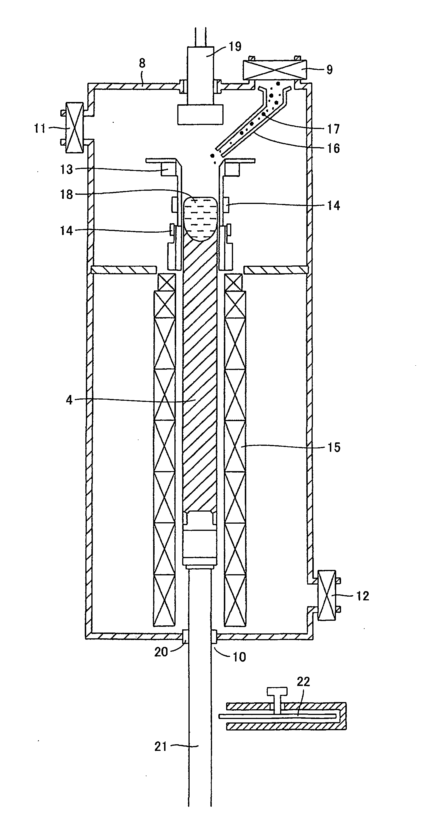
[0063]The sectional dimensions of the ingot as the raw material of the silicon block are set to the following four types: (square section) 345 mm×345 mm, (rectangular sections) 345 mm×450 mm, 345 mm×506 mm, 345 mm×667 mm. In casting, an electromagnetic furnace shown in FIG. 4 is used, and an ingot of overall length 1 m is cast.

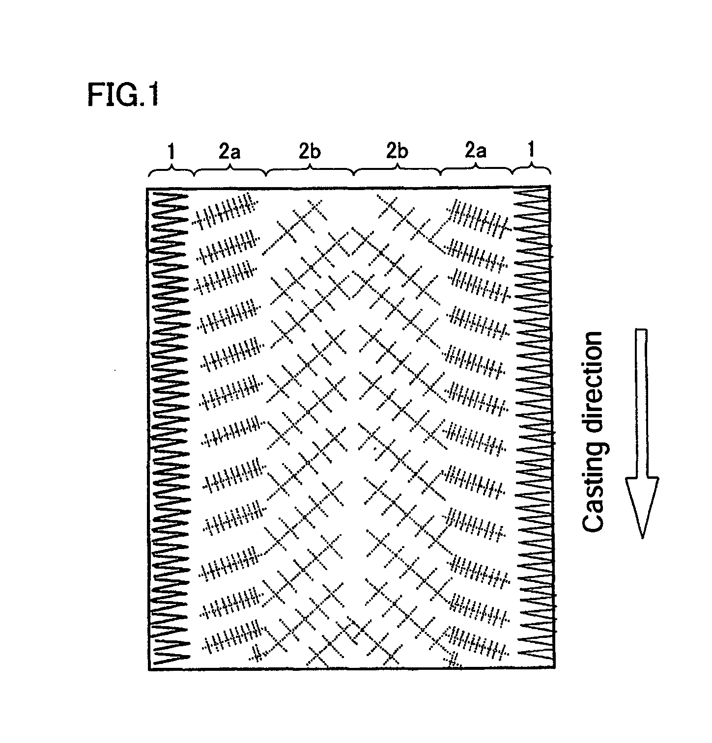
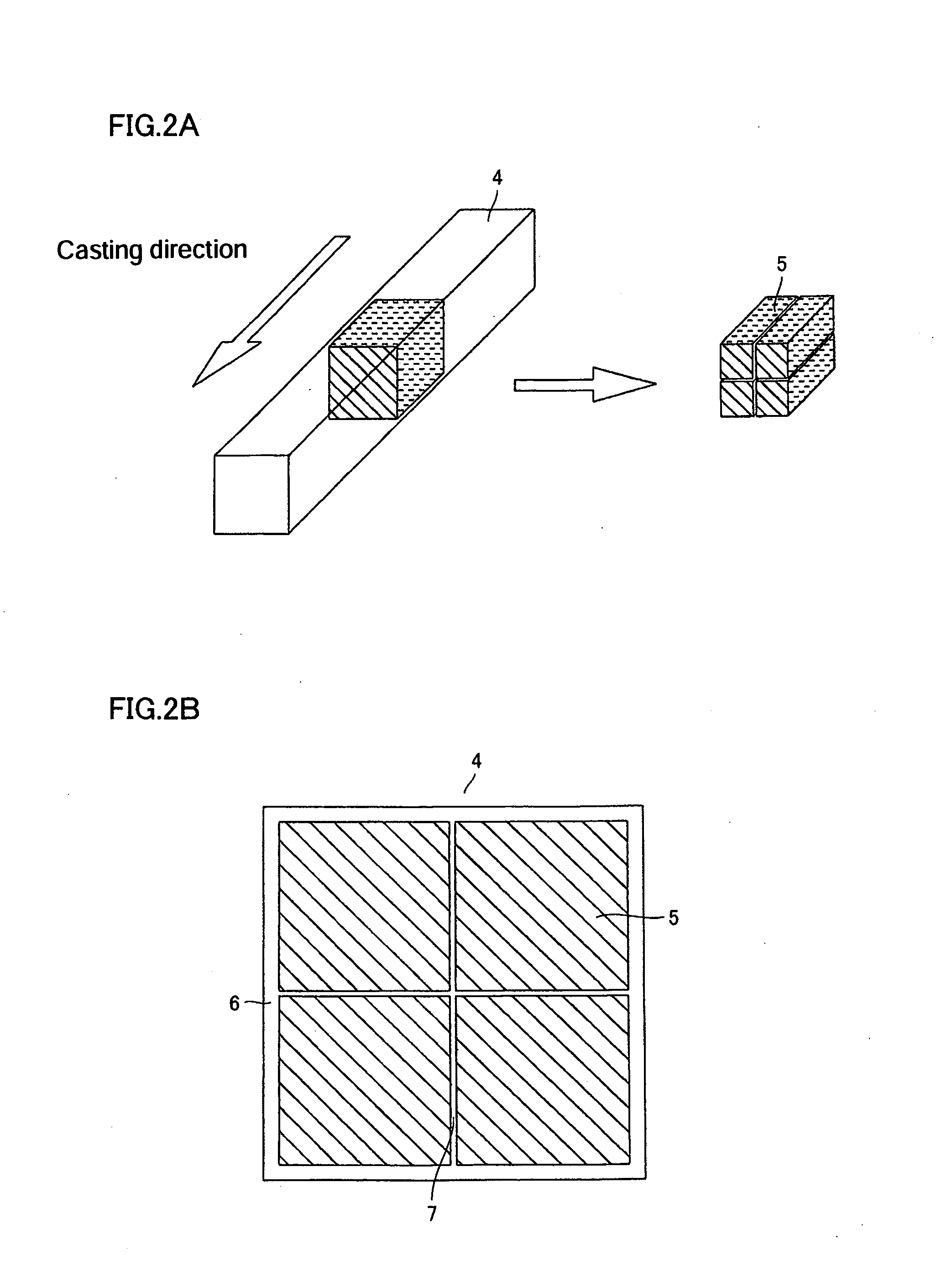
[0064]From the obtained four types of ingots, the silicon blocks of the sectional dimension 156 mm×156 mm are cut out. In any of the ingots, the width of the cutting margin between the silicon blocks is set to 5 mm, and the excision width of the edge is set to 14 mm.

[0065]In Test No. T2 of the inventive example, 4 pieces of silicon blocks of 317 mm in length are cut-out from the ingot with the sectional dimension 345 mm×450 mm, and 6 pieces o...


PUM

PropertyMeasurementUnit
side lengthaaaaaaaaaa
thicknessaaaaaaaaaa
lengthaaaaaaaaaa

Abstract

The present invention includes a method for casting a silicon ingot by using a continuous casting method by means of an electromagnetic induction, and a method for cutting the silicon ingot as a starting material into plural silicon blocks. When the silicon blocks with a square section are cut out, the sectional shape of the silicon ingot is set to be rectangular. Not less than 6 pieces of equal-sized silicon blocks are cut out from the silicon ingot, thereby enabling to enhance the manufacturing efficiency to a great extent. And since the amount of excision of the edge per silicon block is reduced, the production yield can be enhanced. Further, since the proportion of columnar crystals with large grain size inside the ingot can be increased, it becomes possible to enhance the conversion efficiency of a solar battery using the silicon block as a substrate material.

Description

BACKGROUND OF THE INVENTION[0001]1. Field of the Invention[0002]The present invention relates to a casting method of a silicon ingot and a cutting method of the same, more specifically to the casting method and cutting method of the silicon ingot that enhance the manufacturing efficiency, production yield of the silicon ingot and conversion efficiency of a solar battery using a silicon block cut out from the silicon ingot as a substrate material.[0003]2. Description of the Related Art[0004]The majority of solar batteries manufactured these days use silicon crystals as substrate materials for them. The silicon crystal is classified into a monocrystal and a polycrystal. Generally, the solar battery having a high efficiency of energy conversion from incident light energy into electric energy can be obtained by using the monocrystal as the substrate.[0005]Since a high-quality dislocation-free crystal is required for manufacturing a monocrystal silicon, the Czochralski method that pulls ...

Claims


Application Information

Patent Timeline
Patent Type & Authority Applications(United States)
IPC IPC(8): B22D11/126
CPCB22D11/015B22D11/126C30B29/06C30B11/003C30B11/001Y10S117/917
Inventor YOSHIHARA, MITSUOSASATANI, KENICHI
Owner SUMCO CORP
Why Eureka
Try Eureka