Temperature-switched process for wafer backside polymer removal and front side photoresist strip

a technology of photoresist strip and temperature-switched process, which is applied in the direction of electrical discharge tubes, decorative arts, electrical equipment, etc., can solve the problems of affecting the workpiece temperature, so as to achieve the effect of increasing the temperature of the workpi

Inactive Publication Date: 2008-07-31
APPLIED MATERIALS INC
View PDF16 Cites 24 Cited by
  • Summary
  • Abstract
  • Description
  • Claims
  • Application Information

AI Technical Summary

Benefits of technology

[0007]A process is provided for removing backside polymer from a backside of a workpiece and stripping a front side photoresist from a front side of the workpiece in the same chamber. The process includes supporting the workpiece on the backside in a vacuum chamber while leaving at least a peripheral annular portion of a backside of the workpiece exposed. The process first increases the temperature of the workpiece over a range starting at a temperature below about 200 degrees C. The process includes confining the edge of the workpiece so as to establish a gap at the edge on the order of about 1% of the diameter of the chamber, the gap corresponding to a boundary between an upper process zone contain

Problems solved by technology

One problem is that the carbon-containing process gases tend to form polymer precursors in the plasma, which can leave a polymer residue on the front side of the wafer and on the exposed portion of the backside of the wafer, and even some distance under the unexposed portion of the wafer backside.
However, the wafer edge is beveled, and the curved surface on the backside of the wafer edge is also exposed and therefore susceptible to polymer deposition during plasma processing.
Attempting to remove the back-side polymer film by heating and exposing the wafer to an oxygen-rich plasma (during a post-etch polymer removal step) will damage the ultra low-K film by removing carbon from it.
It is generally difficult if not impossible to avoid damaging the ultra low-K (ULK) film beyond the permissible 3 nm depth while exposing the wafer to an oxygen

Method used


Image

  • Temperature-switched process for wafer backside polymer removal and front side photoresist strip
  • Temperature-switched process for wafer backside polymer removal and front side photoresist strip
  • Temperature-switched process for wafer backside polymer removal and front side photoresist strip

Examples


Embodiment Construction

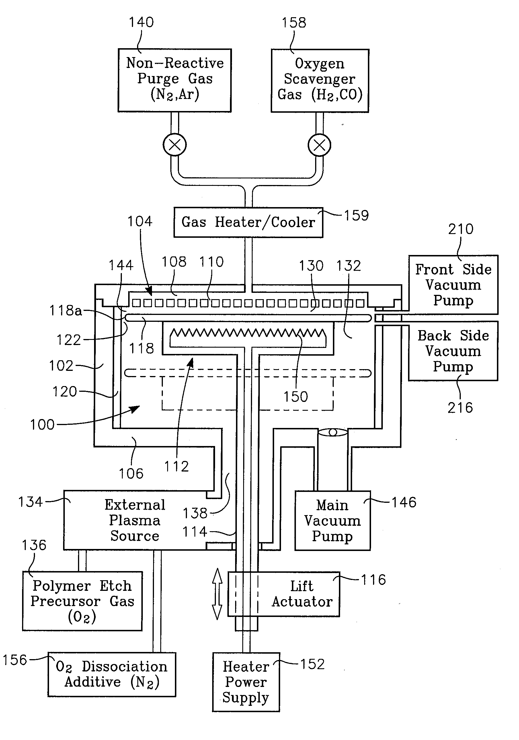
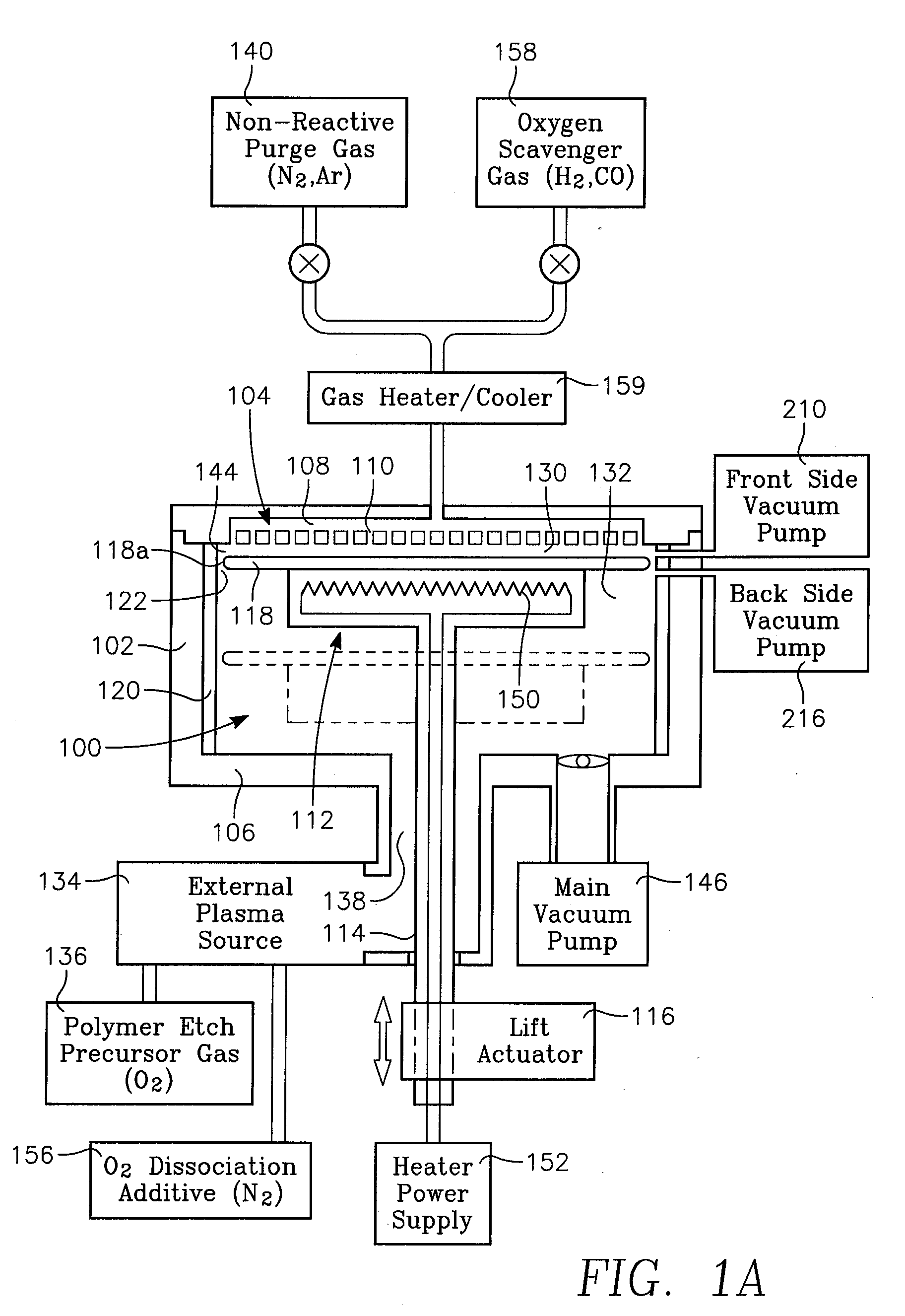
[0035]Exemplary embodiments of the invention pertain to removing polymer from the backside edge of a wafer without damaging critical films, such as an ultra low-K dielectric film, by heating the wafer in a chamber while exposing only the backside of the wafer to polymer etch radicals or plasma by-products, such as atomic or free oxygen, from an external plasma source. The oxygen radicals may be provided by an external plasma source which is supplied with an oxygen-containing gas or vapor, such as O2, H2O, N2O, CO2, or CO, for example. The oxygen-containing gas may be combined or diluted with other gases such as H2, N2 or Ar. Other fluorine-containing gases (such as CF4 or NF3) may be added to allow removal of polymer films that contain other materials (such as Si) and are not etched efficiently in O chemistry alone. The critical films in the thin film structure on the wafer front side are protected from damage by the polymer etch species by pumping purge gases across the wafer front...


PUM

PropertyMeasurementUnit
Fractionaaaaaaaaaa
Lengthaaaaaaaaaa
Lengthaaaaaaaaaa

Abstract

A workpiece is supported on the backside in a vacuum chamber while leaving at least a peripheral annular portion of a backside of the workpiece exposed. The process first increases the temperature of the workpiece starting at a temperature below about 200 degrees C. The edge of the workpiece is confined so as to establish a gap at the edge on the order of about 1% of the diameter of the chamber, the gap corresponding to a boundary between an upper process zone containing the front side and a lower process zone containing the backside. Before the workpiece temperature exceeds about 200 degrees C., backside polymer is removed using a first plasma containing polymer etch species in the lower process zone. After the workpiece temperature reaches about 300 degrees C., photoresist is stripped from the workpiece front side using by-products of a second plasma containing a photoresist strip species in the upper process zone.

Description

CROSS-REFERENCE TO RELATED APPLICATIONS[0001]This application claims the benefit of U.S. Provisional Application Ser. No. 60 / 898,645, filed Jan. 30, 2007.BACKGROUND[0002]Plasma processing of a workpiece or semiconductor wafer, particularly dielectric etch plasma processing, typically employs carbon-containing process gases (e.g., fluorocarbon or fluoro-hydrocarbon gases) that enhance the etch selectivity of dielectric materials, such as silicon dioxide, relative to other materials such as silicon. These processes are used to treat the front (top) side of the wafer on which the microelectronic thin film structures are formed. The opposite (back) side of the wafer is typically unpatterned. One problem is that the carbon-containing process gases tend to form polymer precursors in the plasma, which can leave a polymer residue on the front side of the wafer and on the exposed portion of the backside of the wafer, and even some distance under the unexposed portion of the wafer backside. S...

Claims


Application Information

Patent Timeline
IPC IPC(8): C23F1/00
CPCH01J37/32357H01J37/32366H01L21/68764H01L21/67115H01L21/68728H01L21/67069
Inventor COLLINS, KENNETH S.HANAWA, HIROJINGUYEN, ANDREWBALAKRISHNA, AJITPALAGASHVILI, DAVIDCRUSE, JAMES P.SUN, JENNIFER Y.TODOROW, VALENTIN N.RAUF, SHAHIDRAMASWAMY, KARTIKSCHNEIDER, GERHARD M.YOUSIF, IMADSALINAS, MARTIN JEFFREY
Owner APPLIED MATERIALS INC
Why Eureka
Try Eureka