Photodetector and manufacturing method thereof

Active Publication Date: 2008-07-31
FUJIFILM CORP +1
View PDF4 Cites 2 Cited by
  • Summary
  • Abstract
  • Description
  • Claims
  • Application Information

AI Technical Summary

Benefits of technology

[0037]The first photodetector of the present invention described above may respond in extremely high speed for the following two reasons. Firstly, it has a p-n junction, and the electric field developed between the n-type region and p-type region, in the lateral direction (parallel or substantially parallel to the substrate) is met with the built-in potential of the p-n junction, thereby a depletion layer is extended remarkably and the lateral electric field is strongly enhanced. Secondly, it includes a barrier layer, which blocks a relatively slow movement of carriers from the substrate, so that a high speed lateral movement of carriers becomes predominant. The advantageous effects described above may also be obtained by the second photodetector of the present invention, which is a lateral MSM (Metal-Semiconductor-Metal) photodetector.
[0038]In the photodetectors of the present invention having the aforementioned structures, the active region is not necessarily formed of a high resistance material, unlike the structure described in the non-patent document 2. That is, doping density in the active region is allowed to be, for example, approximately 1×1016 cm−3, thereby the photodetectors may be fabricated easily. In this case, if the p-n junction described above is not formed, the frequency range would be limited to below several hundreds MHz. The photodetectors of the present invention have the p-n junction, so that such limitation in the frequency range may be prevented.

Problems solved by technology

That is, in conventional lateral photodiodes, Si (silicon) forming p-type and n-type regions has low absorption rate for light with wavelengths in the long wavelength range of 650 nm and above, which is often the detection target range in general purpose applications, so that a considerable time is required for movement of carriers, which is one of the impediments to a high speed response.
The structure described in the non-patent document 1, however, requires an additional manufacturing process for providing the deep trench structure, which makes the photodetector costly to manufacture.
The structure described in the non-patent document 2 requires a high resistance material for the active layer, which makes the photodetector difficult to fabricate.
If a high resistance material is not used in the active layer, the whole area of the active layer does not become a depletion layer, so that the carriers need to move by diffusion and a sufficient speed is not obtained.

Method used


Image

  • Photodetector and manufacturing method thereof
  • Photodetector and manufacturing method thereof
  • Photodetector and manufacturing method thereof

Examples


first embodiment

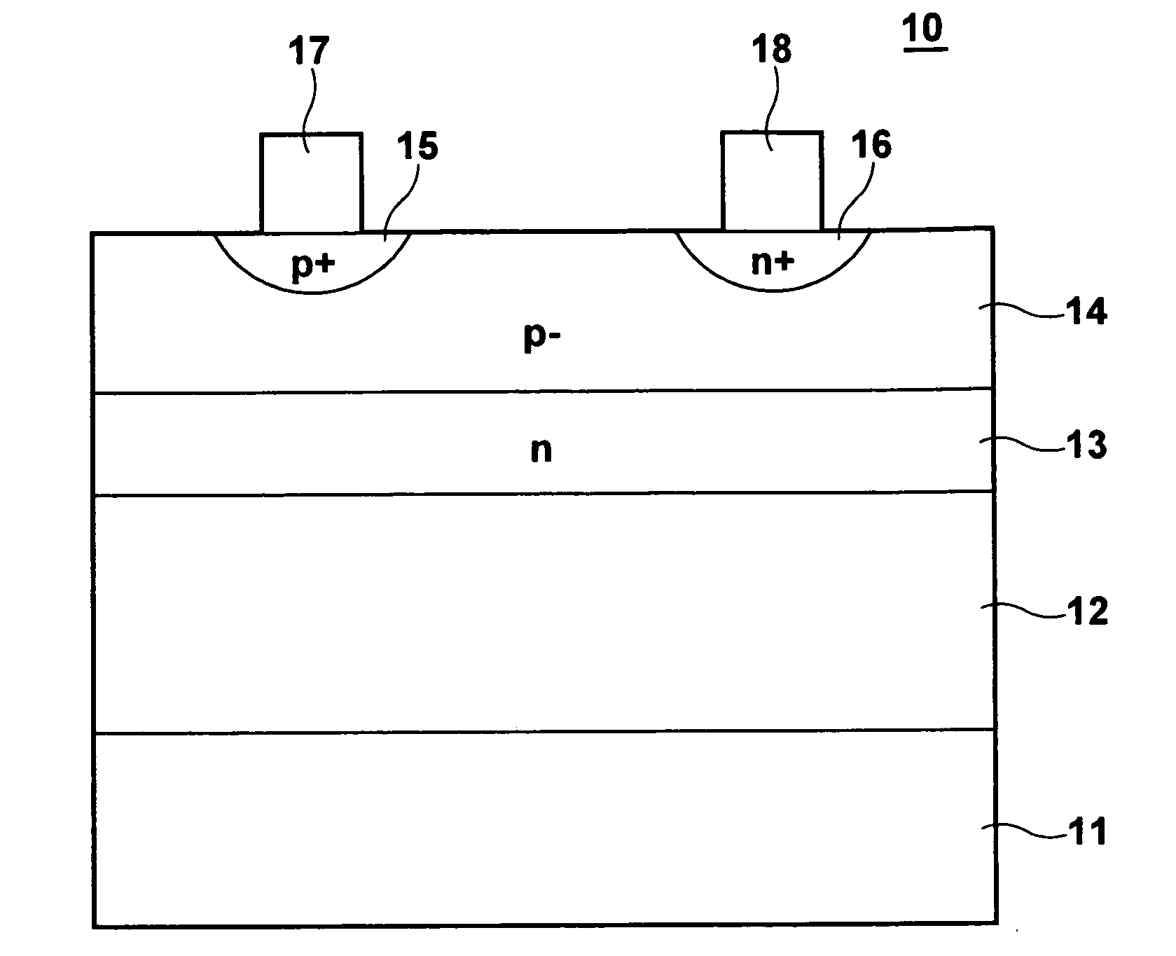
[0055]FIG. 1 schematically illustrates the side shape of the lateral photodetector according to a first embodiment of the present invention. In the present embodiment, the photodetector is, by way of example, a photodiode. As illustrated, the photodiode 10 includes a substrate 11 on which a barrier layer 12, n-type active region (absorption region) 13, and a p-type active region 14 are stacked in this order. Further, a p+ region 15 and an n+ region 16, each having a finger-like shape, are arranged parallel to the surface of the substrate 11 near the surface of the p-type active region 14. A cathode 17 and an anode 18 are connected to the p+ region 15 and n+ region 16 respectively.

[0056]When light is irradiated on the photodiode 10, which has the aforementioned structure, from above in the drawing, carriers (holes and electrons) move between the p+ region 15 and n+ region 16, and a current flows through a load, if it is connected between the cathode 17 and anode 18, so that the light...

second embodiment

[0069]Next, a second embodiment of the present invention will be described. FIG. 9 schematically illustrates the side shape of the lateral photodetector according to the second embodiment of the present invention. In the FIG. 9, components identical to those in FIG. 1 are given the same reference numerals and will not be elaborated upon further here unless otherwise specifically required (the same applies to hereinafter).

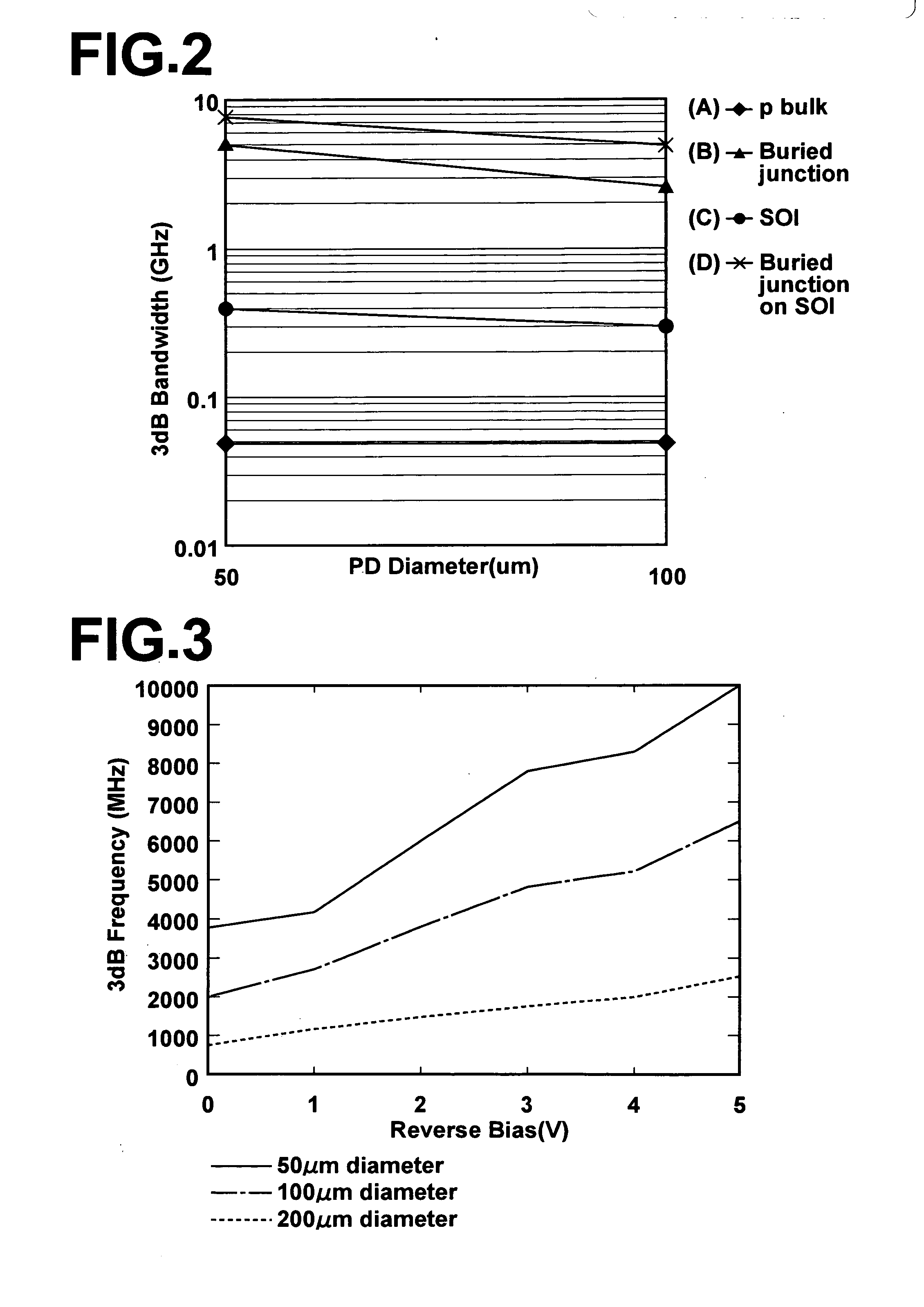
[0070]Here also, the photodetector in the present invention is, by way of example, a photodiode. The photodiode 20 differs from the photodiode 10 shown in FIG. 1 in that it uses a higher doping density substrate as the SOI substrate, thus an n-type (n+-type) active region 23 having a higher doping density that the n-type active region 13 is formed. More specifically, the doping density is 1×1019 cm−3.

[0071]Provision of the n-type (n+-type) active region 23 having such high doping density may provide the effect to extend the depletion layer upward, i.e, opposite to t...

third embodiment

[0072]Next, a third embodiment of the present invention will be described. FIG. 10 illustrates the side shape of the lateral photodetector according to the third embodiment of the present invention. In the present embodiment also, the photodetector is, by way of example, a photodiode. The photodiode 30 differs from the photodiode 10 shown in FIG. 1 in that it includes an n-type active region 33 having varied thickness instead of the planar n-type active layer 13. That is, the n-type active region 33 is formed such that the thickness in the portion under the n+ region 16 and anode 18 is greater than in the portion under the p+ region 15 and cathode 17.

[0073]The photodiode 30 according to the present embodiment may basically provide the identical advantageous effects to those in the first and second embodiments. In addition, it may provide a greater electric field amplifying effect since it has a larger interface area between the n-type active region 33 and p-type active region 14, an...


PUM


Abstract

A lateral photodiode, with improved response speed, includes a semiconductor substrate having active regions, and a p-type region and an n-type region arranged parallel to the surface of the substrate. The active regions are an n-layer and a p-layer respectively, and stacked in the thickness direction of the substrate to form a p-n junction. In addition, a barrier layer, for preventing movement of carriers from the substrate toward the active region, is provided on the side of the active regions toward the substrate.

Description

BACKGROUND OF THE INVENTION[0001]1. Field of the Invention[0002]The present invention relates to a lateral photodetector, and a method for manufacturing the same.[0003]2. Description of the Related Art[0004]Lateral photodiodes, in which p-type and n-type regions are arranged parallel to the surface of the substrate, are known as described for example in Japanese Unexamined Patent Publication No. 5(1993)-175536. FIG. 8 illustrates a basic structure of a lateral photodiode. As illustrated, a semiconductor layer 2 is formed on a substrate 1, and a p-type region 3 and an n-type region 4 are formed parallel to the surface of the substrate 1 within the semiconductor layer 2. Electrodes 8 and 9 are connected to the p-type region 3 and n-type region 4 respectively, and an insulation layer 7 is formed to cover the semiconductor layer 2 from above. In a lateral photodiode having such structure, absorption of light and movement of carriers occur in an area of the semiconductor layer near the s...

Claims


Application Information

Patent Timeline
IPC IPC(8): H01L31/0352H01L31/18
CPCH01L31/103H01L31/109H01L31/1085
Inventor MIYACHI, YUKIYAP. GIZIEWICZ, WOJCIECHMICHEL, JURGENKIMERLING, LIONEL C.
Owner FUJIFILM CORP
Why Eureka
Try Eureka