

Memory Device
a technology of memory and elements, applied in the field of memory elements, can solve the problems of low material efficiency, large amount of energy consumed in the manufacturing process, and product yield drop, and achieve the effects of excellent performance and reliability, simple manufacturing with high yield, and excellent performance and reliability
- Summary
- Abstract
- Description
- Claims
- Application Information
AI Technical Summary
Benefits of technology
Problems solved by technology
Method used
Image

Examples
embodiment mode 1
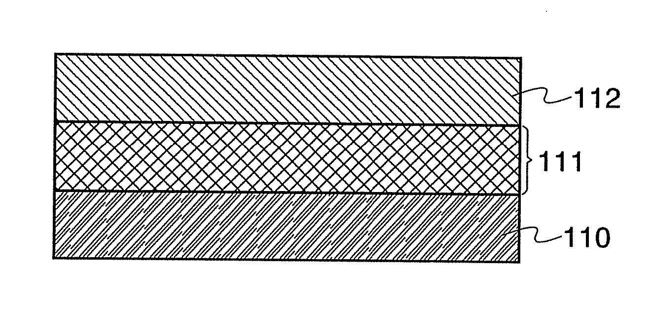
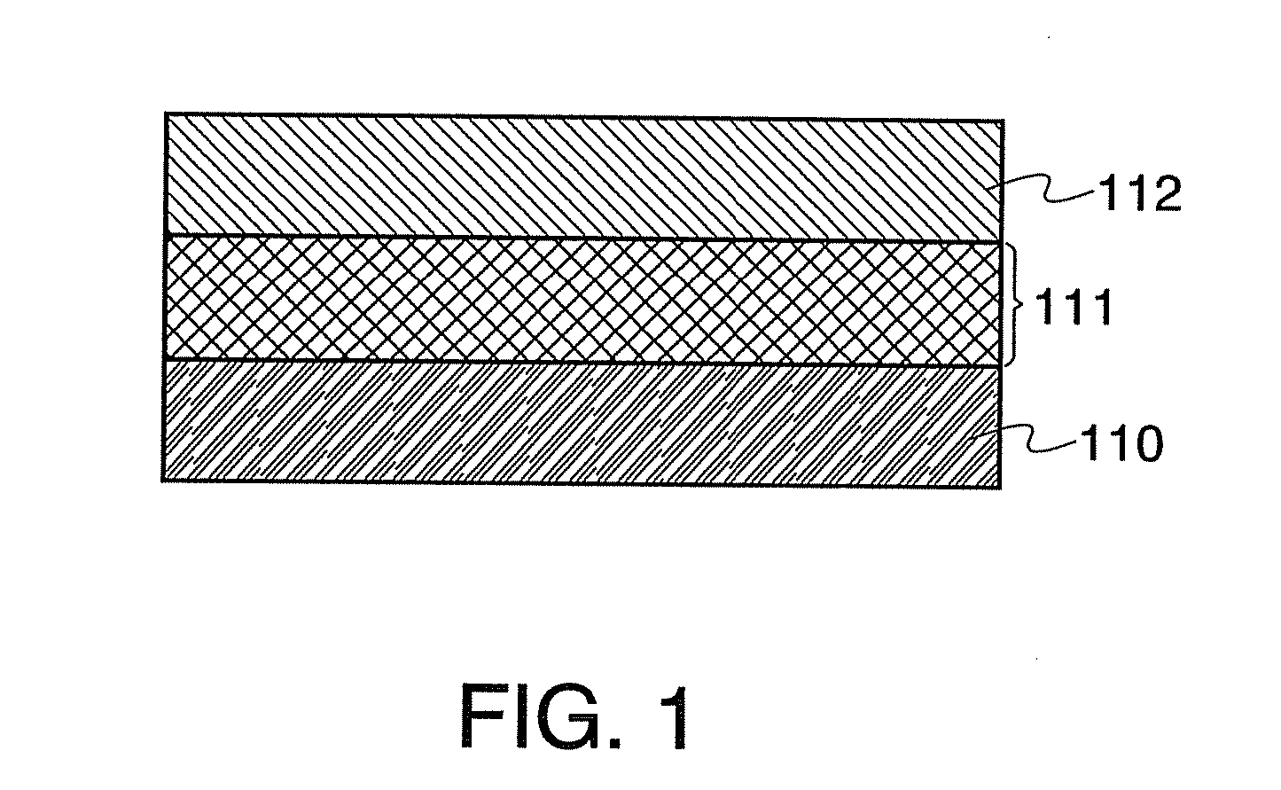
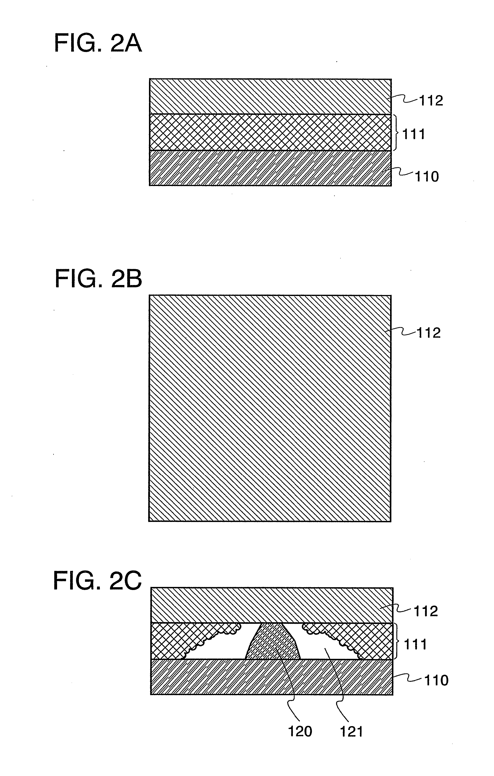
[0051]A structural example of a memory element of the present invention is described with reference to FIG. 1. A memory element shown in FIG. 1 includes a first conductive layer 110, a second conductive layer 112, and a memory layer 111 interposed between the first conductive layer 110 and the second conductive layer 112. The memory layer 111 is formed from nanoparticles of a conductive material each of which is coated with an organic thin film. FIG. 24 is a schematic view of a memory element, in which the organic thin film is denoted by reference numeral 113 and the nanoparticle of a conductive material is denoted by reference numeral 114. As shown in FIG. 24, the second conductive layer 112 is provided over the first conductive layer 110, with a region in which an insulating film formed of the organic thin film 113 and the nanoparticle 114 of a conductive film are alternately disposed interposed therebetween. That is, the first conductive layer 110 is connected to the second condu...
embodiment mode 2
[0091]This embodiment mode will describe a semiconductor device having a memory element of the present invention, typically a memory device, with reference to the drawings. Note that this embodiment mode will show a case where the structure of the memory device is a passive matrix type.
[0092]FIG. 6A shows a structural example of a semiconductor device described in this embodiment mode. A semiconductor device 400 includes a memory cell array 411 where memory elements 401 are arranged in matrix, decoders 412 and 413, a selector 414, and a reading / writing circuit 415. The structure of the semiconductor device 400 which is shown here is only one example and the semiconductor device 400 may also include other circuits such as a sense amplifier, an output circuit, or a buffer.
[0093]The decoders 412 and 413, the selector 414, the reading / writing circuit 415, an interface, and the like may also be formed over a substrate as with the memory element. Alternatively, they may be attached extern...
embodiment mode 3
[0120]This embodiment mode will describe a semiconductor device having a memory element of the present invention with reference to FIGS. 9A to 9C. Specifically, this embodiment mode will describe an active-matrix memory device.
[0121]FIG. 9A shows a structural example of a semiconductor device described in this embodiment mode. A semiconductor device 700 includes a memory cell array 711 where memory cells 701 are arranged in matrix, decoders 712 and 713, a selector 714, and a reading / writing circuit 715. The structure of the semiconductor device 700 which is shown here is only one example and the semiconductor device 700 may also include other circuits such as a sense amplifier, an output circuit, or a buffer.
[0122]The decoders 712 and 713, the selector 714, the reading / writing circuit 715, an interface, and the like may also be formed over a substrate as with a memory element. Alternatively, they may be attached externally as IC chips.
[0123]The memory cell 701 includes a first wirin...
PUM
 Abstract
Description
Claims
Application Information