VCSEL, manufacturing method thereof, optical device, light irradiation device, data processing device, light sending device, optical spatial transmission device, and optical transmission system

a laser diode and vertical cavity technology, applied in the direction of lasers, semiconductor devices, semiconductor lasers, etc., can solve the problems of difficult control of the divergence angle and difficulty in reproducing the diameter of the oxidized apertur

Active Publication Date: 2008-08-07
FUJIFILM BUSINESS INNOVATION CORP
View PDF5 Cites 28 Cited by
  • Summary
  • Abstract
  • Description
  • Claims
  • Application Information

AI Technical Summary

Benefits of technology

[0006]When a VCSEL is used as a light source in optical communication or optical storage, it is required that divergence angle or far field pattern (FFP) of laser light emitted from the VCSEL be smaller than a certain value. If divergence angle becomes greater, spot diameter becomes greater, thereby error occurrence in optical communication may increase, or resolution in reading or writing data from or to a storage media may be reduced.

Problems solved by technology

Especially if the diameter of an oxidized aperture becomes as small as in single-mode, it is difficult to reproduce the diameter of the oxidized aperture, which makes it difficult to control divergence angle.

Method used


Image

  • VCSEL, manufacturing method thereof, optical device, light irradiation device, data processing device, light sending device, optical spatial transmission device, and optical transmission system
  • VCSEL, manufacturing method thereof, optical device, light irradiation device, data processing device, light sending device, optical spatial transmission device, and optical transmission system
  • VCSEL, manufacturing method thereof, optical device, light irradiation device, data processing device, light sending device, optical spatial transmission device, and optical transmission system

Examples


Embodiment Construction

[0030]Referring to the accompanying drawings, exemplary embodiments for implementing the present invention will be now described.

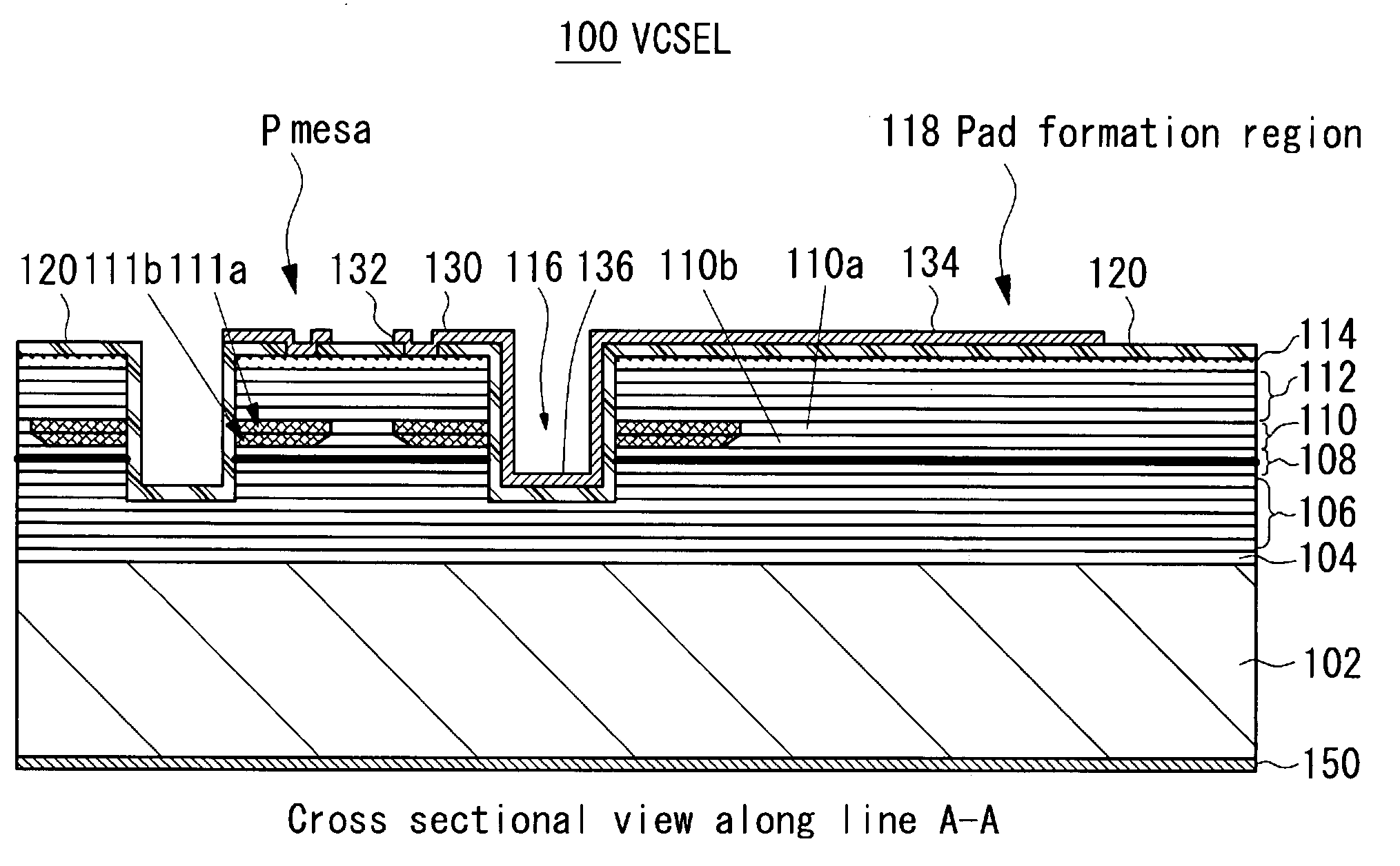
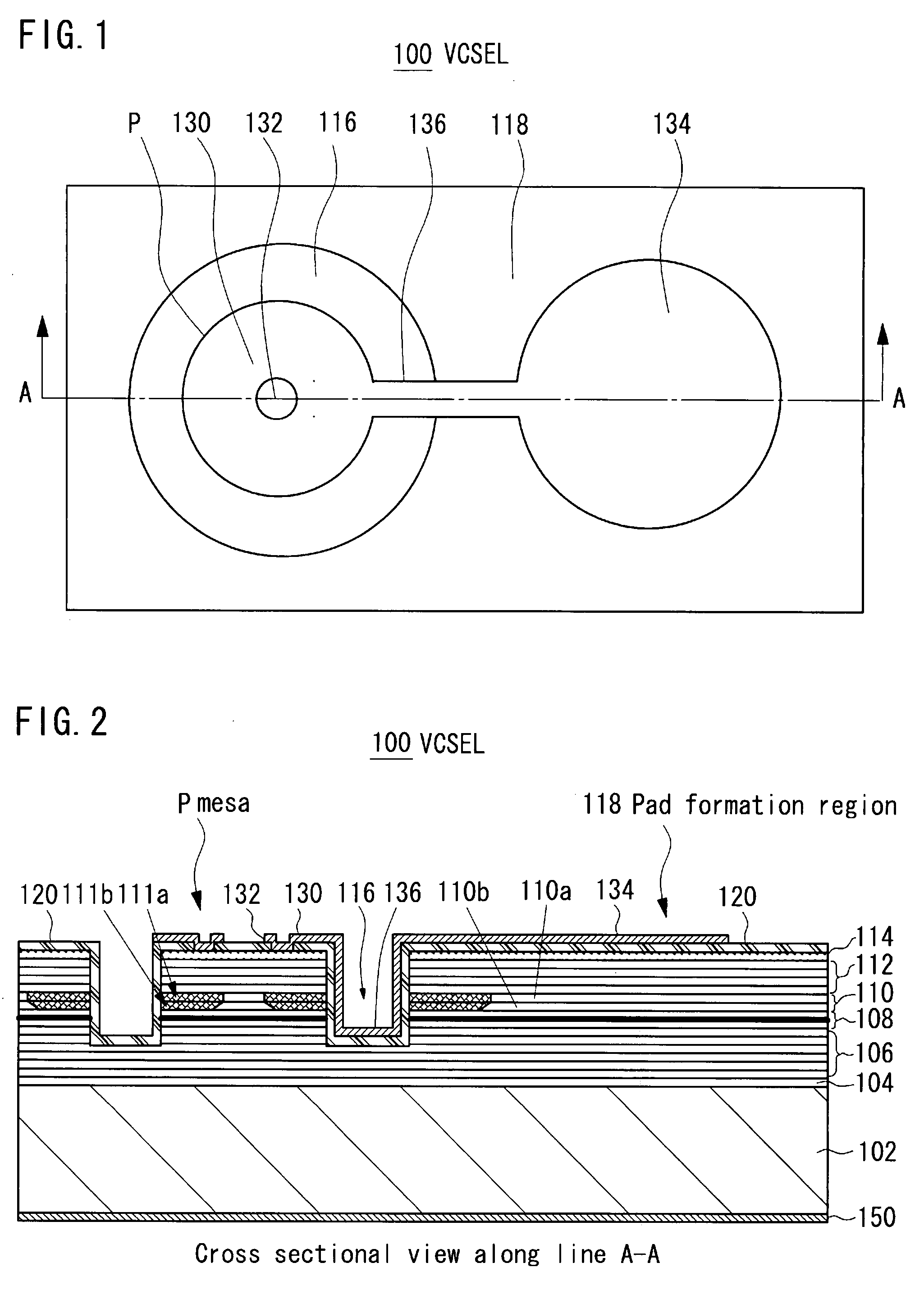
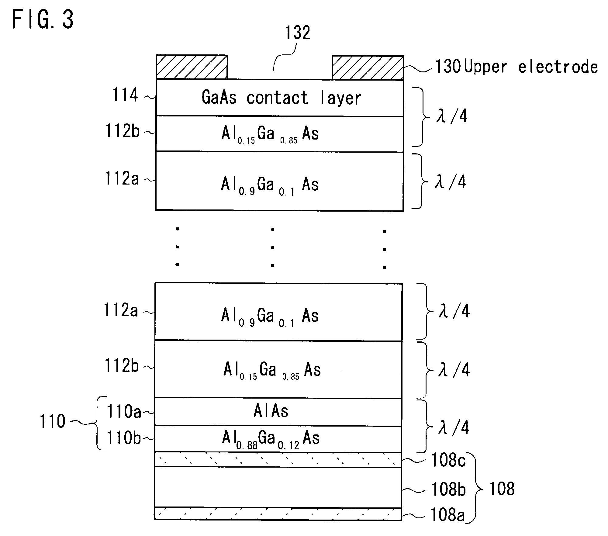
[0031]FIG. 1 is a plan view of a VCSEL according to an example of the invention, and FIG. 2 is a cross sectional view taken along line A-A of FIG. 1. As shown in FIG. 1 and FIG. 2, a VCSEL 100 includes an n-side electrode 150 on the back surface of an n-type GaAs substrate 102. Stacked on the substrate 102 are semiconductor layers that include the n-type GaAs buffer layer 104, a lower DBR (Distributed Bragg Reflector) 106 made of an n-type AlGaAs semiconductor multilayer, an active region 108, a current confining layer 110 made of two layers, a p-type AlAs layer and a p-type AlGaAs layer, an upper DBR 112 made of a p-type AlGaAs semiconductor multilayer, and a p-type GaAs contact layer 114.

[0032]To the substrate 102, a ring-shaped groove 116 is formed by etching the semiconductor layers such that the groove 116 has a depth from the contact layer 114 to a p...


PUM


Abstract

A VCSEL includes a first conductivity-type first semiconductor mirror layer on a substrate, an active region thereon, a second conductivity-type second semiconductor mirror layer thereon, and a current confining layer in proximity to the active region. A mesa structure is formed such that at least a side surface of the current confining layer is exposed. The current confining layer includes a first semiconductor layer having an Al-composition and a second semiconductor layer having an Al-composition and being formed nearer to the active region than the first semiconductor layer does. Al concentration of the first semiconductor layer is higher than that of the second semiconductor layer. When oscillation wavelength of laser light is λ, optical thickness being sum of the thickness of the first and second semiconductor layers is λ / 4. The first and second semiconductor layers are selectively oxidized from the side surface of the mesa structure.

Description

CROSS-REFERENCE TO RELATED APPLICATIONS[0001]This application is based on and claims priority under 35 USC 119 from Japanese Patent Application No. 2007-024089 filed Feb. 2, 2007.BACKGROUND[0002]1. Technical Field[0003]The present invention relates to a Vertical-Cavity Surface-Emitting Laser diode (hereinafter referred to as VCSEL), an optical device, a light irradiation device, a data processing device, a light sending device, an optical spatial transmission device, an optical transmission system, and a method for manufacturing a VCSEL.[0004]2. Related Art[0005]In technical fields such as optical communication or optical storage, there has been a growing interest in VCSELs. VCSELs have excellent characteristics that edge-emitting semiconductor lasers do not have. For example, VCSELs are characterized by lower threshold current and smaller power consumption. With a VCSEL, a round light spot can be easily obtained. Also, evaluation can be performed while VCSELs are on a wafer, and li...

Claims


Application Information

Patent Timeline
Patent Type & Authority Applications(United States)
IPC IPC(8): H01S5/183H01L33/00H01S5/187
CPCB82Y20/00H01S5/02284H01S5/02288H01S5/0425H01S2301/18H01S5/18333H01S5/18358H01S5/3432H01S5/18311H01S5/04252H01S5/04254H01S5/18394H01S5/02253H01S5/02251
Inventor YOSHIKAWA, MASAHIROYAMAMOTO, MASATERUKONDO, TAKASHI
Owner FUJIFILM BUSINESS INNOVATION CORP
Why Eureka
Try Eureka