Nanotube array electronic devices

Inactive Publication Date: 2008-08-14
NANO ELECTRONICS & PHOTONIC DEVICES & CIRCUITS
View PDF16 Cites 29 Cited by
  • Summary
  • Abstract
  • Description
  • Claims
  • Application Information

AI Technical Summary

Benefits of technology

[0013]To build a nanotube array ballistic transistor (NABT), according to the present invention, one has to provide two contacts to each nanotube in the array. The first contact is made as a metal electrode deposited on an insulating substrate, like glass. It is followed by deposition on the metal electrode of small pads of a catalytic metal, such as Ni, Co or F

Problems solved by technology

In this configuration, parallel placement of multiple identical nanotubes to enhance the outp

Method used


Image

  • Nanotube array electronic devices
  • Nanotube array electronic devices
  • Nanotube array electronic devices

Examples


Embodiment Construction
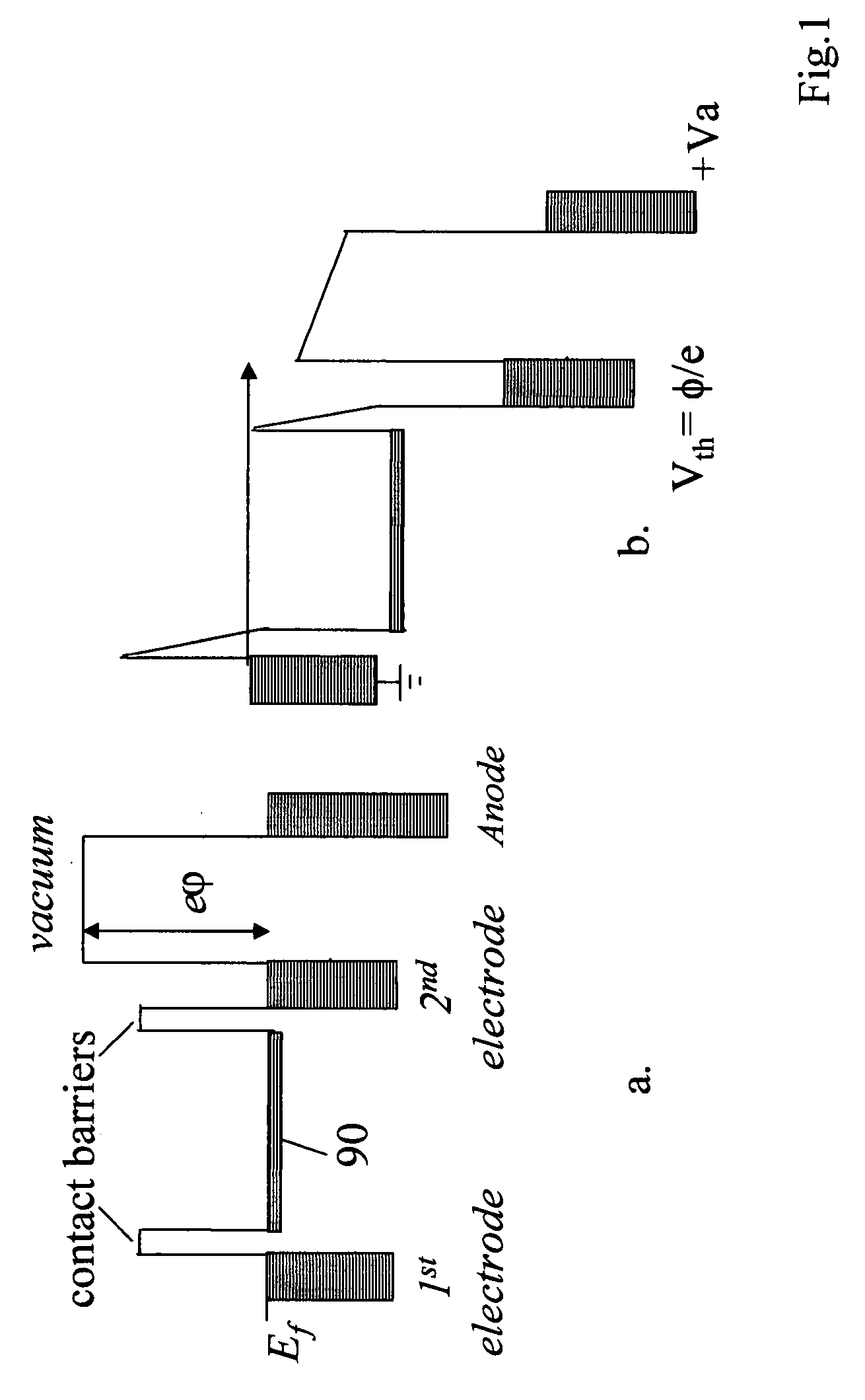
1. The NABTs

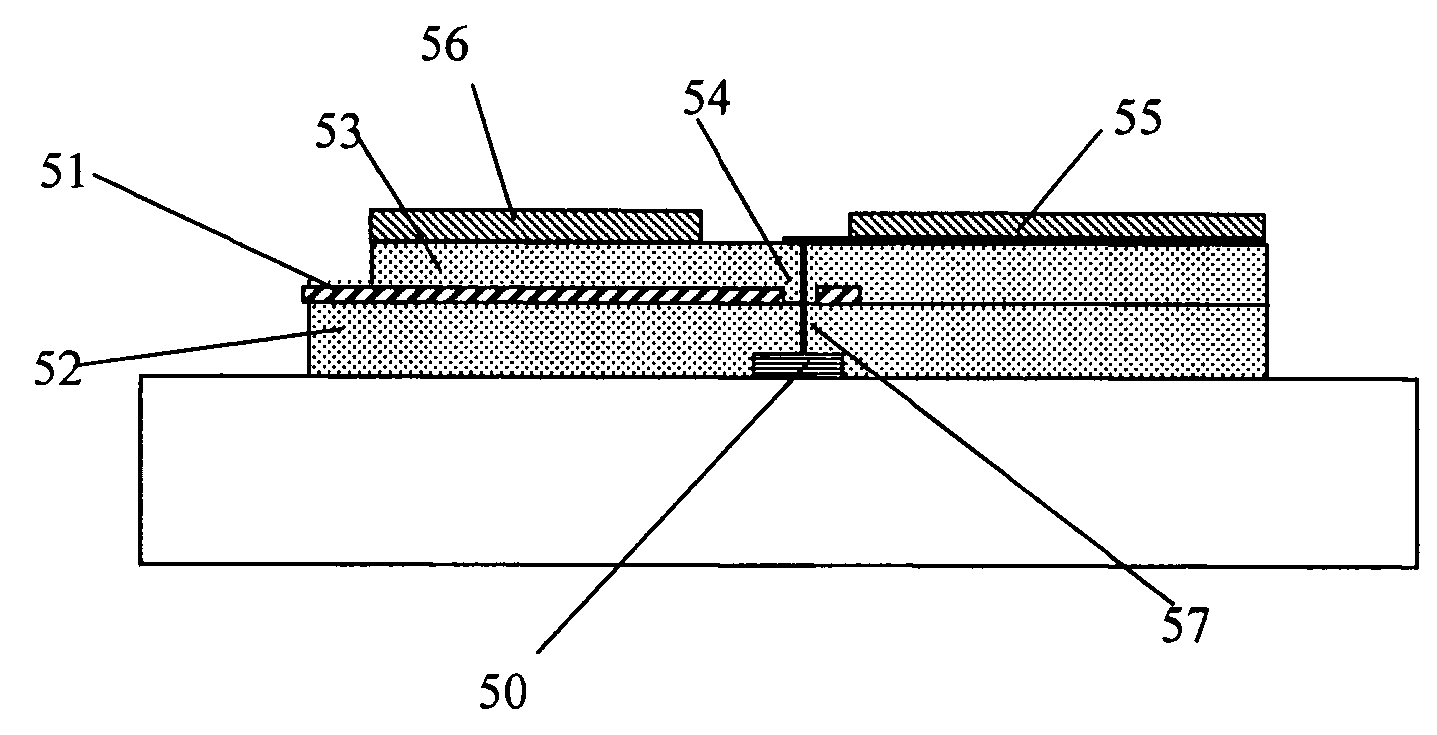
[0023]FIG. 3a shows the cross-sectional view of the NABT structure. The device is made on the insulating substrate (glass) 31 using planar layer deposition technology. The first metal layer 32 is deposited in the shape of a stripe (normally to the drawing plane) and serves as a cathode electrode, on which the nanotube array will be grown. Before the nanotube growth, small pads of catalytic material (not shown), such as Ni, Fe or Co, are deposited on the metal layer 32 to activate the process of growth. After the nanotube growth, an insulator film 36, such as SiO2 or SiOx, having the thickness smaller than the nanotube height, is deposited. It is followed by polishing of the top surface to cut off the nanotubes ends and thus to both expose the nanotube tips and provide a flat platform for further processing. The grown nanotubes are shown in FIG. 3b as a linear array 33 normal to the substrate plane.

[0024]The next processing step is unique, since it relates to formation of...


PUM


Abstract

The Nanotube Array Ballistic Transistors are disclosed, wherein the ballistic (without collisions) electron propagation along the nanotubes, grown normally to the substrate plane on the common metal electrode, is used for a new class of hybrid (solid state/vacuum) electronic devices. In the disclosed transistors, the array of nanotubes emits electrons into vacuum when electrons gain sufficient energy inside the nanotubes due to ballistic electron movement under the voltage applied to the nanotube ends.
In the disclosed devices, planar layer deposition technology is used to form multilayer structures and attach two electrodes to the nanotubes ends.
The ballistic transistor can also be used for making a new type of electron-emission display when a phosphor layer is deposited on the anode electrode.
The non-ballistic nanotube array transistor, employing field-induced electron emission and the same planar layer deposition technique, is also disclosed, the device being considered to be a transistor approaching terahertz frequency range of operation.

Description

FIELD OF THE INVENTION[0001]The invention relates to carbon nanotube array ballistic electron sources, as well as transistors and diodes employing array of grown nanotubes.BACKGROUND OF THE INVENTION[0002]The carbon nanotubes (CNT) possess unique properties due to extremely small nanotube diameter (˜1 nm for a single walled CNT,) which gives rise to a strong two-dimensional quantization of the energy spectrum. As a result, the electron scattering is largely suppressed and the electrons move along the nanotube ballistically, i.e. without collisions and loss of energy, while the nanotube resistance is essentially controlled by the contact resistances. The minimum contact resistance is determined by the quantum contact resistance of 6.5 kOhm (per contact).[0003]In the previous patent U.S. Pat. No. 7,102,157, the ballistic electron propagation along the nanotube was utilized to disclose a vacuum electron emitter, in which electrons under the potential difference between the contacts V a...

Claims


Application Information

Patent Timeline
IPC IPC(8): H01L29/06H01J1/62
CPCB82Y10/00H01L29/0665H01L51/057H01L29/0676H01L51/0048H01L29/0673H10K85/221H10K10/491
Inventor KASTALSKY, ALEXANDER
Owner NANO ELECTRONICS & PHOTONIC DEVICES & CIRCUITS
Why Eureka
Try Eureka