
Mobile circuit robust against input voltage change

a mobile circuit and input voltage technology, applied in logic circuits using specific components, logic circuit coupling/interface arrangement, pulse technique, etc., can solve the problems of compound inability to apply, and low price of silicon semiconductor based rtd devices,

Inactive Publication Date: 2008-08-28
SAMSUNG ELECTRONICS CO LTD
View PDF7 Cites 10 Cited by
  • Summary
  • Abstract
  • Description
  • Claims
  • Application Information

AI Technical Summary

Benefits of technology

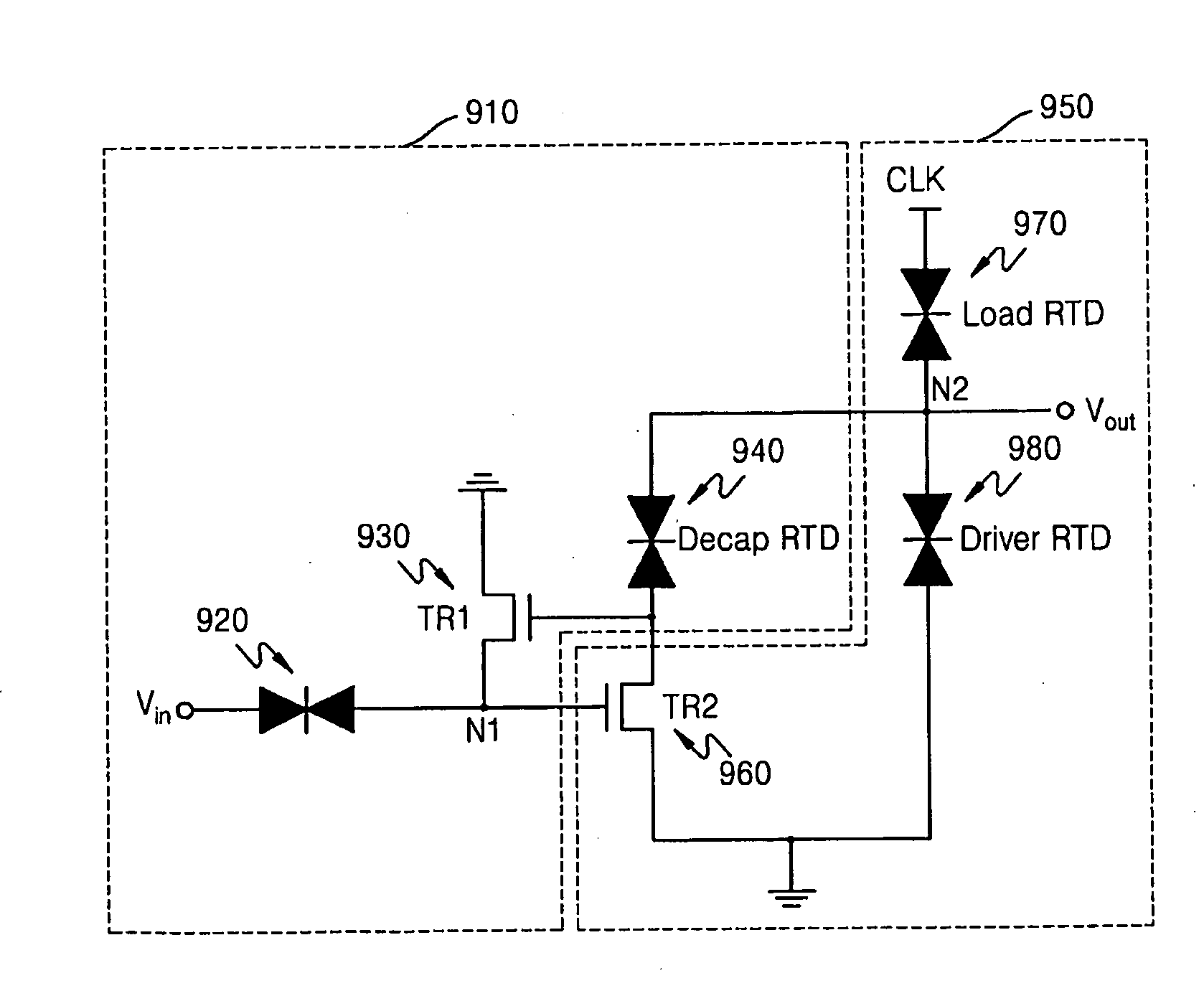
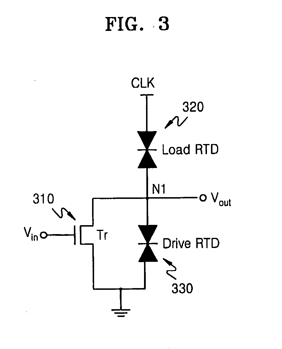
[0015]The present invention provides a monostable-bistable transition logic element (MOBILE) circuit that can provide a stable output independently of an input data change in consideration of peak-to-valley current ratio (PVCR) characteristics of a resonant tunneling diode (RTD).

Problems solved by technology

However, when the minimum linewidth is below 10 nm, electrons are greatly affected by the quantum-mechanical operation and thus the classical principle, which simply treats an electron as an independent electrical particle, cannot be applied as it is now.
The silicon semiconductor based RTD device is low in price and compatible with the conventional CMOS process, but cannot be used in high-frequency circuits.
In contrast, the compound semiconductor based RTD device can be used in high-frequency circuits, but is high in price and incompatible with the conventional CMOS process.
However, the silicon semiconductor based RTD device is small in terms of peak-to-valley current ratio (PVCR) and thus is difficult to use for a wide range of technical fields.
In particular, when the MOBILE circuit is constructed using the silicon semiconductor based RTD device and an input voltage margin is small, the number of stable points decreases due to the small-PVCR characteristics of the RTD device, which causes a malfunction in the MOBILE circuit.

Method used


Image

  • Mobile circuit robust against input voltage change
  • Mobile circuit robust against input voltage change
  • Mobile circuit robust against input voltage change

Examples


Embodiment Construction

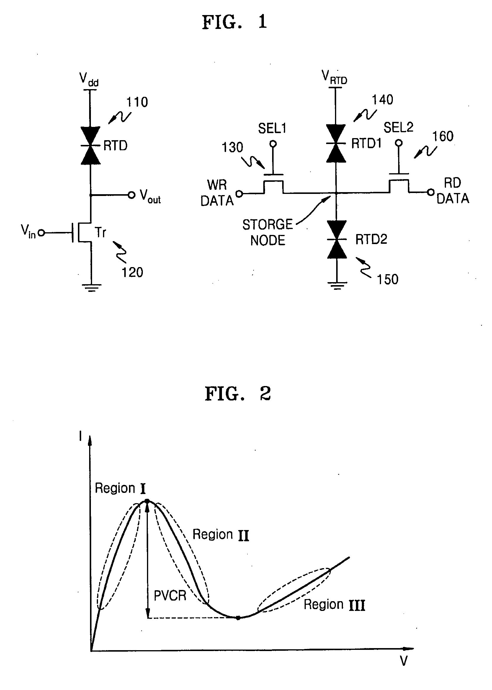
[0035]FIG. 1 illustrates logic devices constructed using resonant tunneling diodes (RTDs).

[0036]Referring to FIG. 1, the left diagram in FIG. 1 illustrates an inverter constructed using an RTD, while the right diagram in FIG. 1 illustrates a static random access memory (SRAM) constructed using RTDs.

[0037]Unlike a conventional inverter constructed using a P-type metal oxide semiconductor field effect transistor (MOSFET) and an N-type MOSFET, the inverter illustrated in FIG. 1 is constructed using an RTD 110 and an N-type MOSFET 120, which can increase the pull-up speed and reduce the power consumption. In addition, unlike a conventional SRAM that is constructed using four or six transistors, the SRAM illustrated in FIG. 1 is constructed using two RTDs 140 and 150 and two N-type MOSFETs 130 and 160, which can reduce the circuit area and the power consumption.

[0038]FIG. 2 is a graph illustrating the I-V characteristics of an RTD.

[0039]Referring to FIG. 2, an I-V curve of the RTD can be...


PUM


Abstract

An inverting flip-flop (F / F) circuit type monostable-bistable transition logic element (MOBILE) circuit that uses resonant tunneling diodes (RTDs) and can prevent a malfunction caused by low peak-to-valley current ratio (PVCR) characteristics of the RTD includes an input data conversion circuit and an inverting F / F circuit. The input data conversion circuit receives input data and converts a logic level of the input data according to a logic level of output data of the MOBILE circuit. The inverting F / F circuit inverts a logic level of data output from the input data conversion circuit and outputs the output data. Accordingly, even when a logic level of input data changes from LOW to HIGH, the logic level of output data can be maintained HIGH in the inverting F / F type MOBILE circuit constructed using silicon semiconductor based RTDs with a small PVCR. Therefore, it is possible to enhance the performance of the inverting F / F circuit type MOBILE circuit.

Description

CROSS-REFERENCE TO RELATED PATENT APPLICATION[0001]This application claims the benefit of Korean Patent Application No. 10-2007-0018098, filed on Feb. 22, 2007, in the Korean Intellectual Property Office, the contents of which are incorporated herein in their entirety by reference.BACKGROUND OF THE INVENTION[0002]1. Field of the Invention[0003]The present invention relates to a monostable-bistable transition logic element (MOBILE) circuit, and more particularly, to an inverting flip-flop (F / F) circuit type MOBILE circuit that uses resonant tunneling diodes (RTDs) and can prevent a malfunction caused by small peak-to-valley current ratio (PVCR) characteristics of the RTD.[0004]2. Description of the Related Art[0005]The semiconductor industry has steadily grown from the late 20th century. The core technology of the semiconductor industry can be broadly classified into the miniaturization and the integration of semiconductor devices. Thanks to the miniaturization of semiconductor devic...

Claims


Application Information

Patent Timeline
Patent Type & Authority Applications(United States)
IPC IPC(8): H03K19/10H03K19/0175
CPCH03K19/00315B60H1/00564B60H1/00821
Inventor YOON, MYOUNG-HOONLEE, SANG-HOON
Owner SAMSUNG ELECTRONICS CO LTD
Learn More