Semiconductor device and method for fabricating the same

a semiconductor and semiconductor technology, applied in the field of semiconductor devices, can solve the problems of poor adhesion at the interface between the cap film and the copper wiring, increase the resistance of the wiring, and deterioration of the reliability of the circuit by electromigration, so as to achieve stable fabrication of the semiconductor and highly reliable metal wiring

Inactive Publication Date: 2008-09-04
FUJITSU LTD
View PDF2 Cites 34 Cited by
  • Summary
  • Abstract
  • Description
  • Claims
  • Application Information

AI Technical Summary

Benefits of technology

[0011]Therefore, one possible object is to provide a semiconductor device including highly reliable metal wirings having resistance to electromigration.
[0012]Another possible object is to provide a method for stably fabricating a semiconductor device including highly reliable metal wirings.

Problems solved by technology

The electromigration causes a void or a hillock in the wiring, resulting in an increase in the resistance of the wiring, the breaking of the wiring, a short circuit, or the like.
That is to say, the electromigration deteriorates the reliability of a circuit.
Adhesion at an interface between the cap film and the copper wiring is poorer than adhesion at an interface between the barrier metal and the copper wiring.
It is considered that diffusion of copper atoms contained in the copper wiring tends to occur at the interface between the cap film and the copper wiring where adhesion is poor.
In such a situation, it may be impossible to adequately suppress the electromigration only by taking a material for the cap film into consideration and changing the properties of the interface between the cap film and the copper wiring in the above way.
As a result, forming the cap film by the use of SiN makes high-speed operation of the device impossible.
However, it is not always easy to selectively form a metal cap film in that way over narrow-pitch wirings in a next generation semiconductor device.
Accordingly, under the present situation a problem still exists from the viewpoint of mass production.

Method used


Image

  • Semiconductor device and method for fabricating the same
  • Semiconductor device and method for fabricating the same
  • Semiconductor device and method for fabricating the same

Examples


example 1

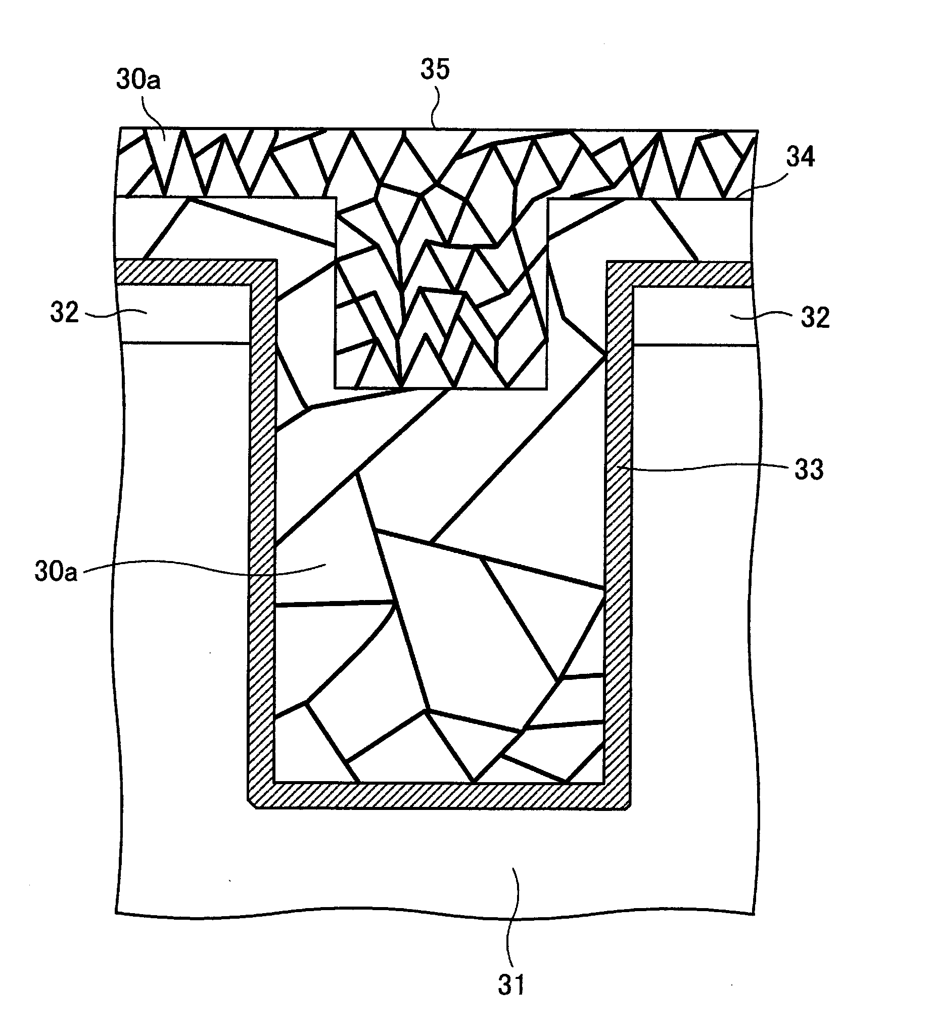
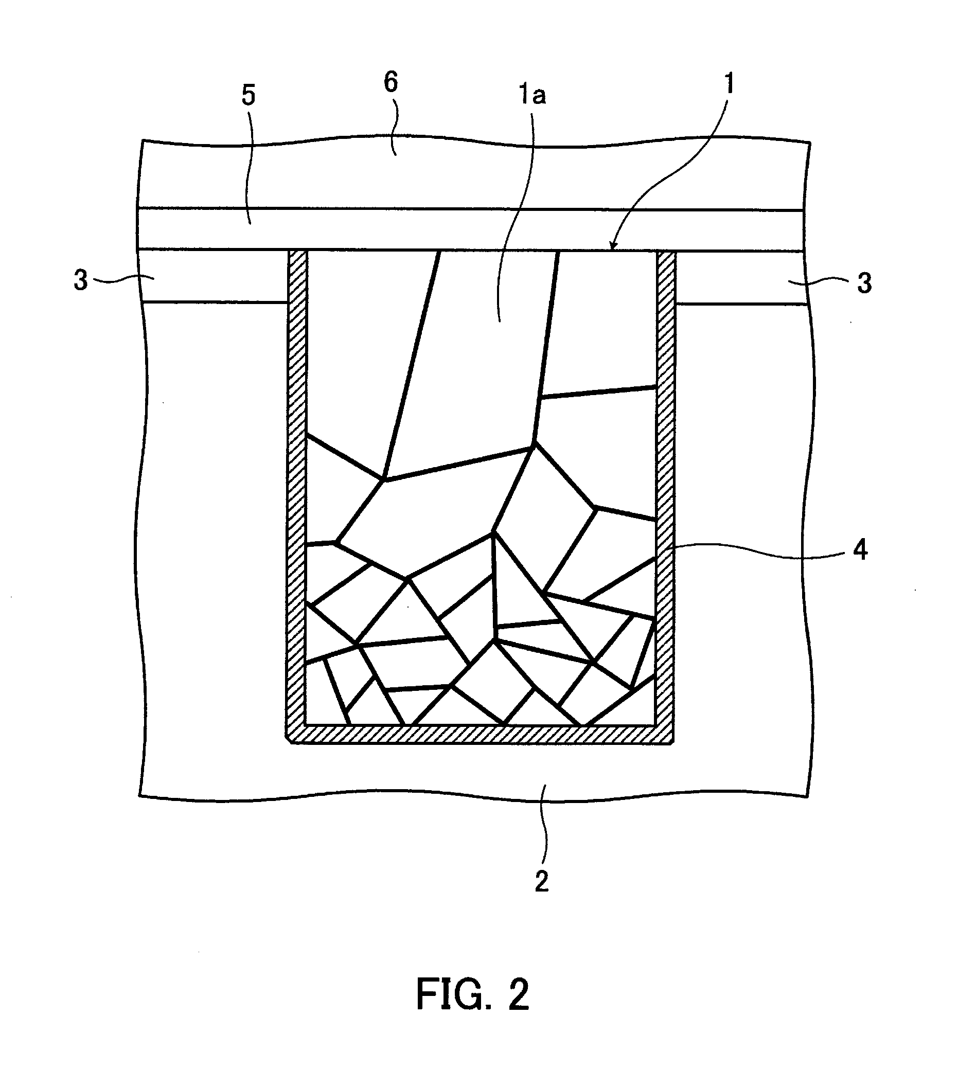
[0085]An example using the method in which the condition of electric current density is controlled at electroplating time will be described. FIGS. 10A through 10J are sectional views showing steps for forming a copper wiring. A transistor portion is not shown. The steps will be described in order.

[0086]FIG. 10A is a fragmentary schematic sectional view showing the step of forming an interlayer dielectric and a hard mask.

[0087]A low dielectric constant (low-k) film of silicon oxide carbide (SiOC) with a thickness of about 250 nm is deposited first over a foundation insulating film 51 of SiO2 formed over a silicon substrate 50 by the CVD method to form an interlayer dielectric 52. A hard mask 53 with a thickness of about 50 nm is formed over the interlayer dielectric 52.

[0088]FIG. 10B is a fragmentary schematic sectional view showing the step of forming a groove.

[0089]After the interlayer dielectric 52 and the hard mask 53 are formed, a groove 54 with a width of 100 to 1000 nm for a l...

example 2

[0114]An example using the method in which ion implantation is used will be described.

[0115]The same steps that are shown in FIGS. 10A through 10C of the above example 1 are performed for forming a copper wiring. In a next electroplating step of FIG. 10D for forming a lower layer copper wiring, the conventional method is used for forming a copper film 56. That is to say, electric current density is set to about 3 mA / cm2 in the beginning stage of the electroplating in which a lower portion and lower sidewall portions of a groove 54 shown in FIG. 10C are filled in, and is then increased gradually. The electric current density is set to 20 mA / cm2 in the middle stage of the electroplating in which a central portion of the groove 54 is filled in. After that, the electric current density is not changed until the groove 54 is completely filled in.

[0116]Planarization is then performed by the CMP in the same way that is shown in FIG. 10. After that, ion implantation is performed before a cap...

example 3

[0124]An example using the method in which the electroplating step is divided into two parts will be described.

[0125]The same steps that are shown in FIGS. 10A through 10C of the above example 1 are performed for forming a copper wiring. In a next electroplating step of FIG. 10D for forming a lower layer copper wiring, electroplating is performed twice under different conditions.

[0126]First, electric current density is set to about 3 mA / cm2 in the beginning stage of first electroplating. The electric current density is gradually increased and is set to 20 mA / cm2 in the middle stage of the first electroplating. By doing so, a lower portion, lower sidewall portions, and a central portion of a groove 54 shown in FIG. 10C are filled in. The first electroplating is ended at this point of time. In this state heat treatment is performed at a temperature of about 350° C. As a result, copper grains grow and their grain sizes increase. After the heat treatment is performed, second electroplat...


PUM

PropertyMeasurementUnit
widthaaaaaaaaaa
widthaaaaaaaaaa
widthaaaaaaaaaa

Abstract

A semiconductor device in which the resistance of a copper wiring to electromigration is increased. The copper wiring is formed so that copper grains will be comparatively large in a central portion of the copper wiring and so that copper grains will be comparatively small in an upper portion and a lower portion of the metal wiring. The copper wiring having this structure is formed by a damascene method. This structure can be formed by controlling electric current density at electroplating time. With the copper wiring having this structure, it is easier for an electric current to run through the central portion than to run through the upper portion. As a result, the diffusion of copper atoms in the upper portion is suppressed and therefore the diffusion of copper atoms from an interface between the copper wiring and a cap film is suppressed.

Description

CROSS-REFERENCE TO RELATED APPLICATIONS[0001]This application is based upon and claims the benefits of priority from the prior Japanese Patent Application No. 2007-034997, filed on Feb. 15, 2007, the entire contents of which are incorporated herein by reference.BACKGROUND OF THE INVENTION[0002](1) Field of the Invention[0003]This invention relates to a semiconductor device and a method for fabricating the semiconductor device and, more particularly, to a semiconductor device having metal wirings of copper (Cu) or the like and a method for fabricating such a semiconductor device.[0004](2) Description of the Related Art[0005]With an increase in the integration levels of silicon (Si) semiconductor devices and a reduction in the sizes of chips, wirings formed in these semiconductor devices have become thinner and the number of wiring layers formed in these semiconductor devices has increased. With devices in which a half pitch is 65 nm, for example, the minimum wiring width is about 100...

Claims


Application Information

Patent Timeline
Patent Type & Authority Applications(United States)
IPC IPC(8): H01L23/532H01L21/4763
CPCH01L21/2885H01L21/76877H01L21/76886H01L23/53223Y10T428/24917H01L23/53295H01L2924/0002H01L23/53238H01L2924/00H01L21/76807H01L21/76834H01L21/7685H01L2924/01029
Inventor SUZUKI, TAKASHIKITADA, HIDEKI
Owner FUJITSU LTD
Why Eureka
Try Eureka