

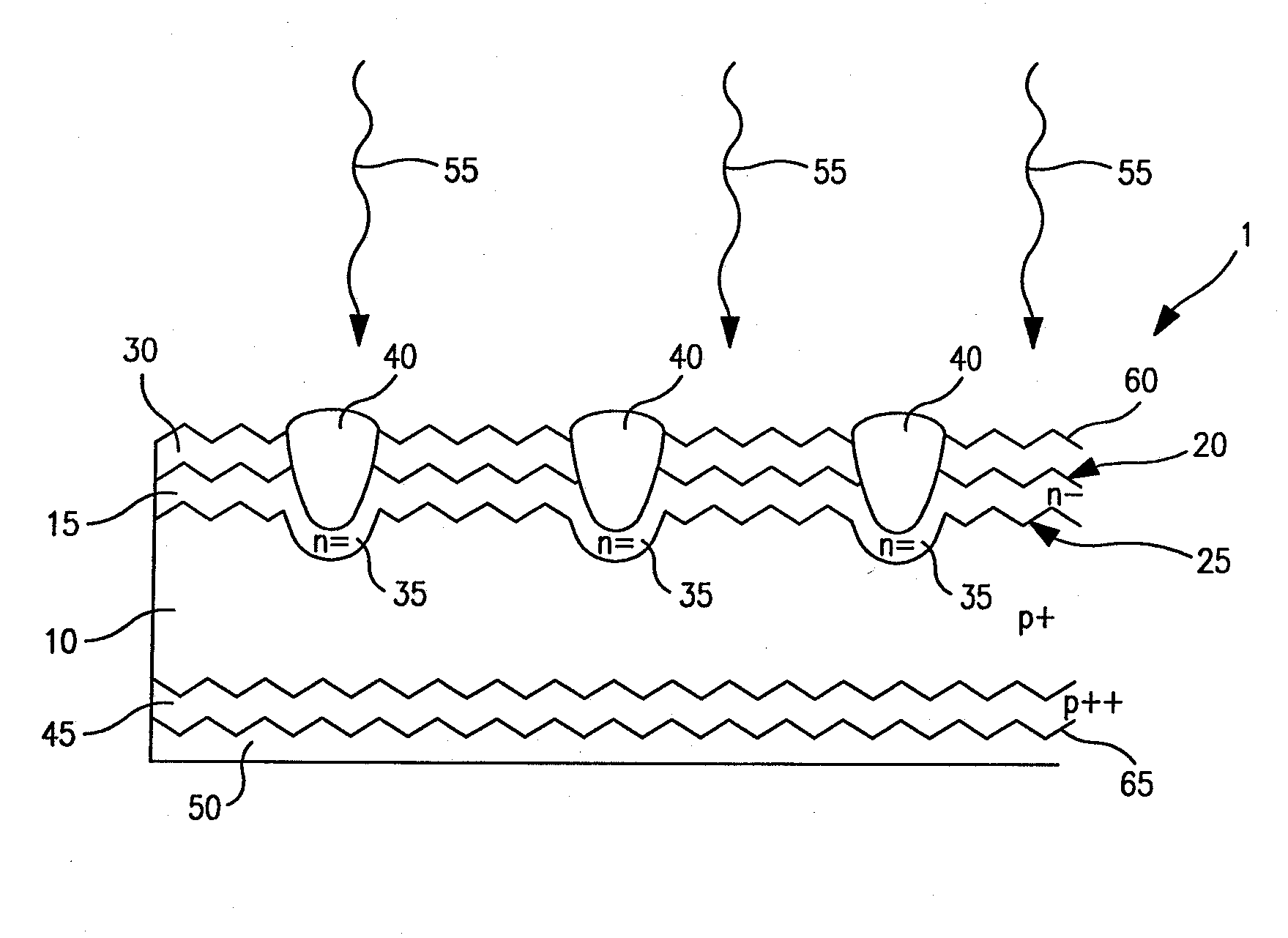
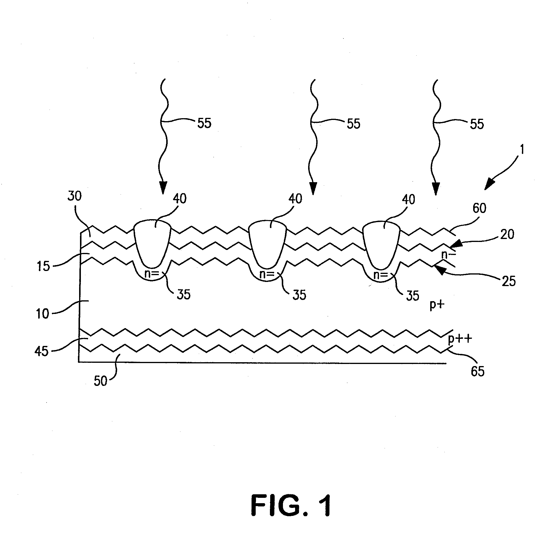
Process for Manufacturing Photovoltaic Cells
a photovoltaic cell and manufacturing technology, applied in the field of photovoltaic cell manufacturing, can solve the problems of undesirable cell efficiency reduction, adversely affecting the formation of the back surface field, and the method used to obtain suitable semiconductor wafers
- Summary
- Abstract
- Description
- Claims
- Application Information
AI Technical Summary
Problems solved by technology
Method used
Image

Examples
examples 1 and 2
OF THE INVENTION
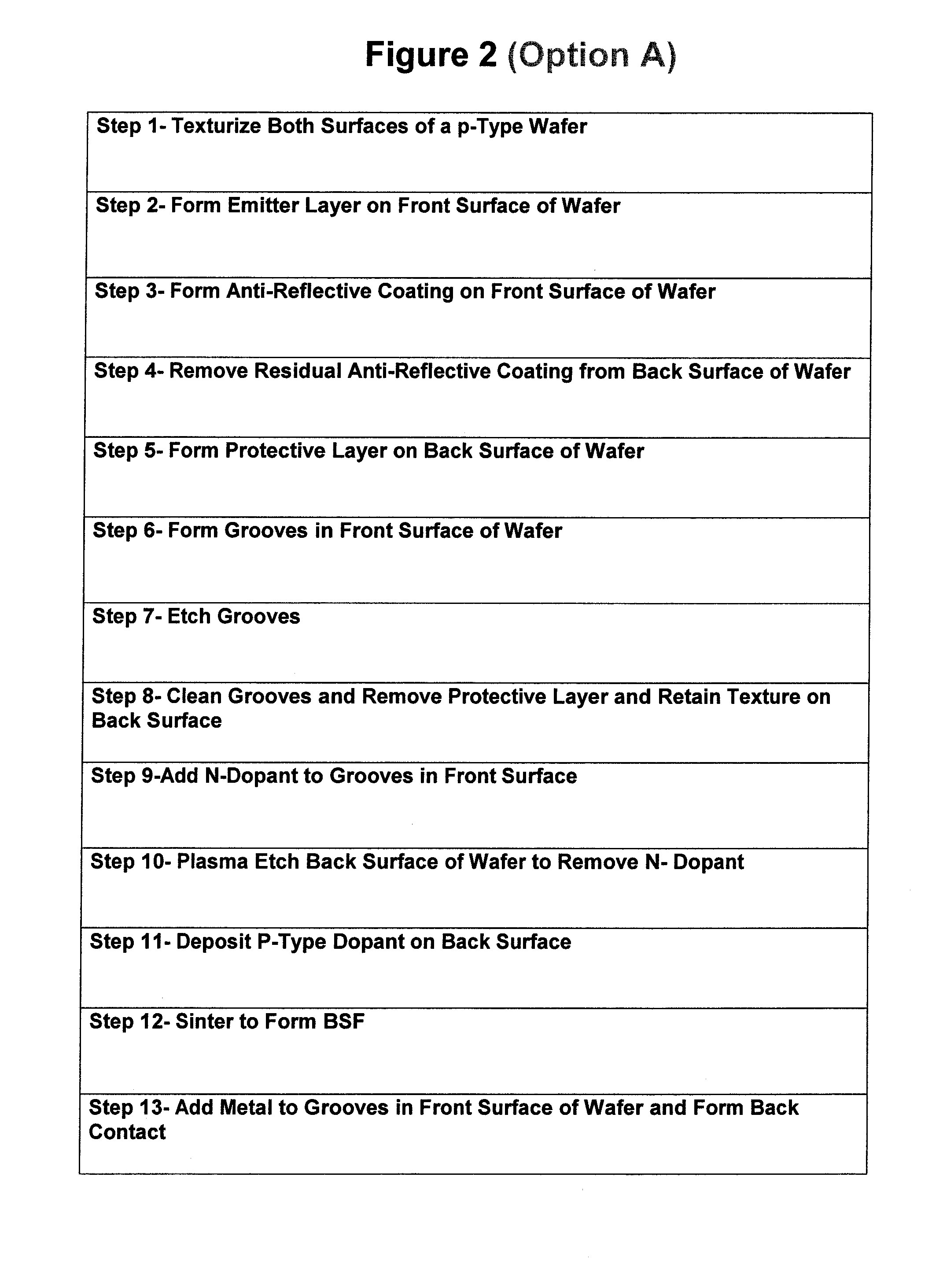
[0071]Examples 1 and 2 describe making photovoltaic cells in accordance with two embodiments of this invention.
[0072]1. Starting Material
[0073]The silicon wafers used were conventional Cz silicon wafers doped p-type with boron to a resistivity of 1.2 ohm.cm and grown with [100] crystal planes parallel to the wafer surface. The wafer dimensions were 127 millimeters square with rounded corners of a diameter 165 millimeters, and had a area of 154.3 cm2. The wafer thickness was 300 micrometers. Such wafers are commercially available, for example, from Bayer Solar GmbH, PV Silicon GmbH or Pillar.
[0074]2. Wafer Surface Preparation
[0075]The wafers were anisotropically “texture” etched in a solution of sodium hydroxide and propanol at a temperature of 85° C. and cleaned by subsequent immersions in hydrofluoric acid and hydrochloric acid with intermediate and final rinsing in de-ionized water followed by drying.
[0076]3. Phosphorus Doping
[0077]Wafers were placed in pairs (touc...
PUM
 Abstract
Description
Claims
Application Information