High efficiency rectifier

a high-efficiency, rectifier technology, applied in semiconductor devices, diodes, electrical devices, etc., can solve the problems of inconvenient use, inconvenient use, and inability to meet the requirements of low-voltage applications, and achieve the effect of reducing the number of trench schottky

Active Publication Date: 2008-09-11
DIODES INC
View PDF4 Cites 16 Cited by
  • Summary
  • Abstract
  • Description
  • Claims
  • Application Information

AI Technical Summary

Benefits of technology

[0007]The present invention overcomes the above-discussed problems and limitations by providing an improved semiconductor rectifier device. Broadly characterized, the device comprises a layer of silicon which has been supersaturated with a dopant of a first conductivity type, a body region of the first conductivity type located substantially below and adjacent to the layer of supersaturated silicon, a drift region of a second conductivity type located substantially below and adjacent to the body region, and a substrate of the second conductivity type located substantially below the drift region.

Problems solved by technology

Unfortunately, Schottky barrier rectifiers suffer from undesirably high reverse leakage current when operating at elevated temperatures.
In addition to these high voltage applications, there is an increasing demand for low voltage applications, for which conventional trench Schottky is not well suited.
Unfortunately, it also results in a significant reduction in the area available for the Schottky barrier because the trench may consume as much as 50% of the area available on the chip.
Unfortunately, this device suffers from its parasitic N+ / P / N bipolar structure resulting in reduced dV / dt performance.

Method used


Image

  • High efficiency rectifier
  • High efficiency rectifier
  • High efficiency rectifier

Examples


Embodiment Construction

.

BRIEF DESCRIPTION OF THE DRAWING FIGURES

[0012]The present invention is described herein with reference to the following drawing figures, with greater emphasis being placed on clarity rather than scale:

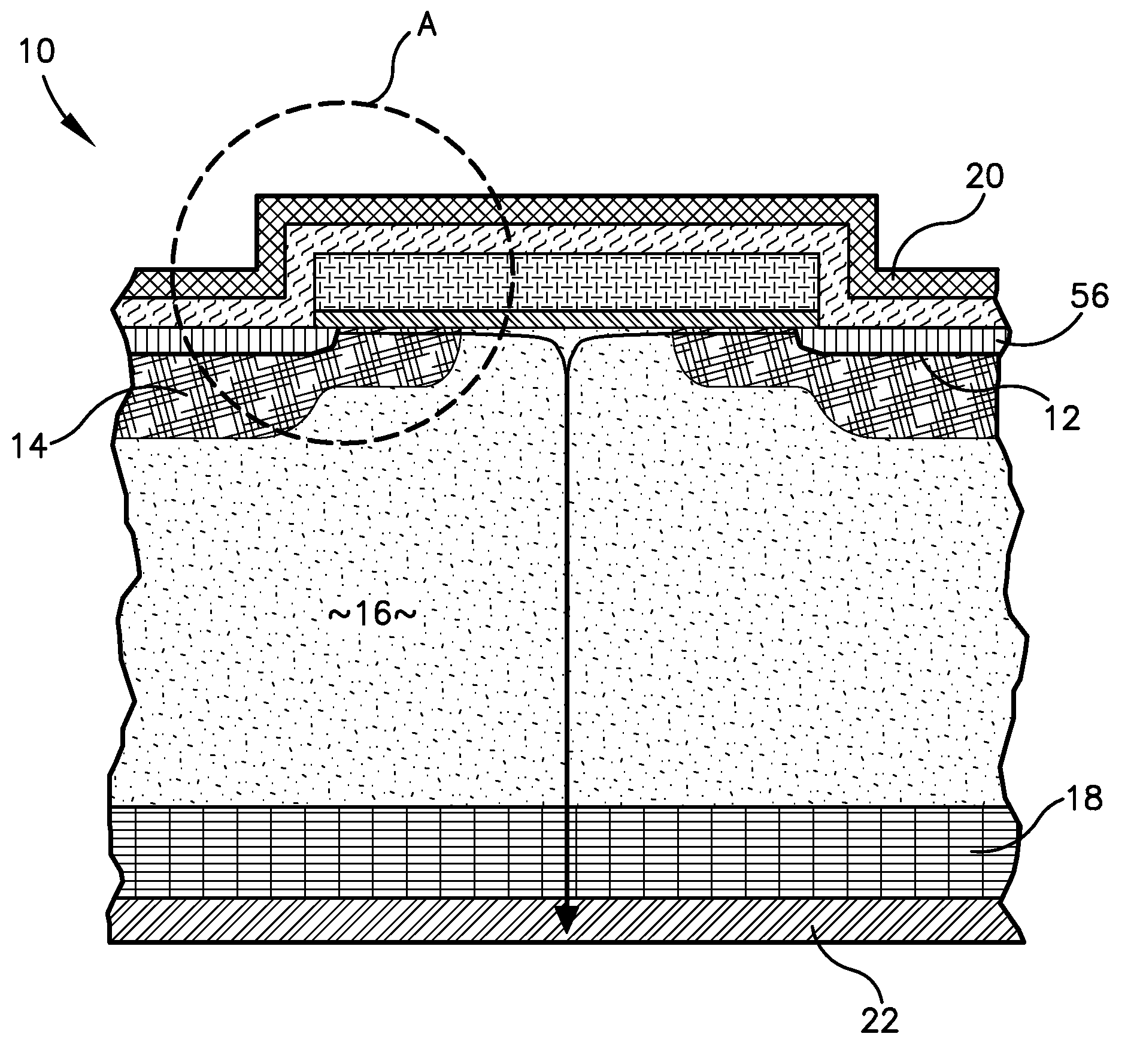
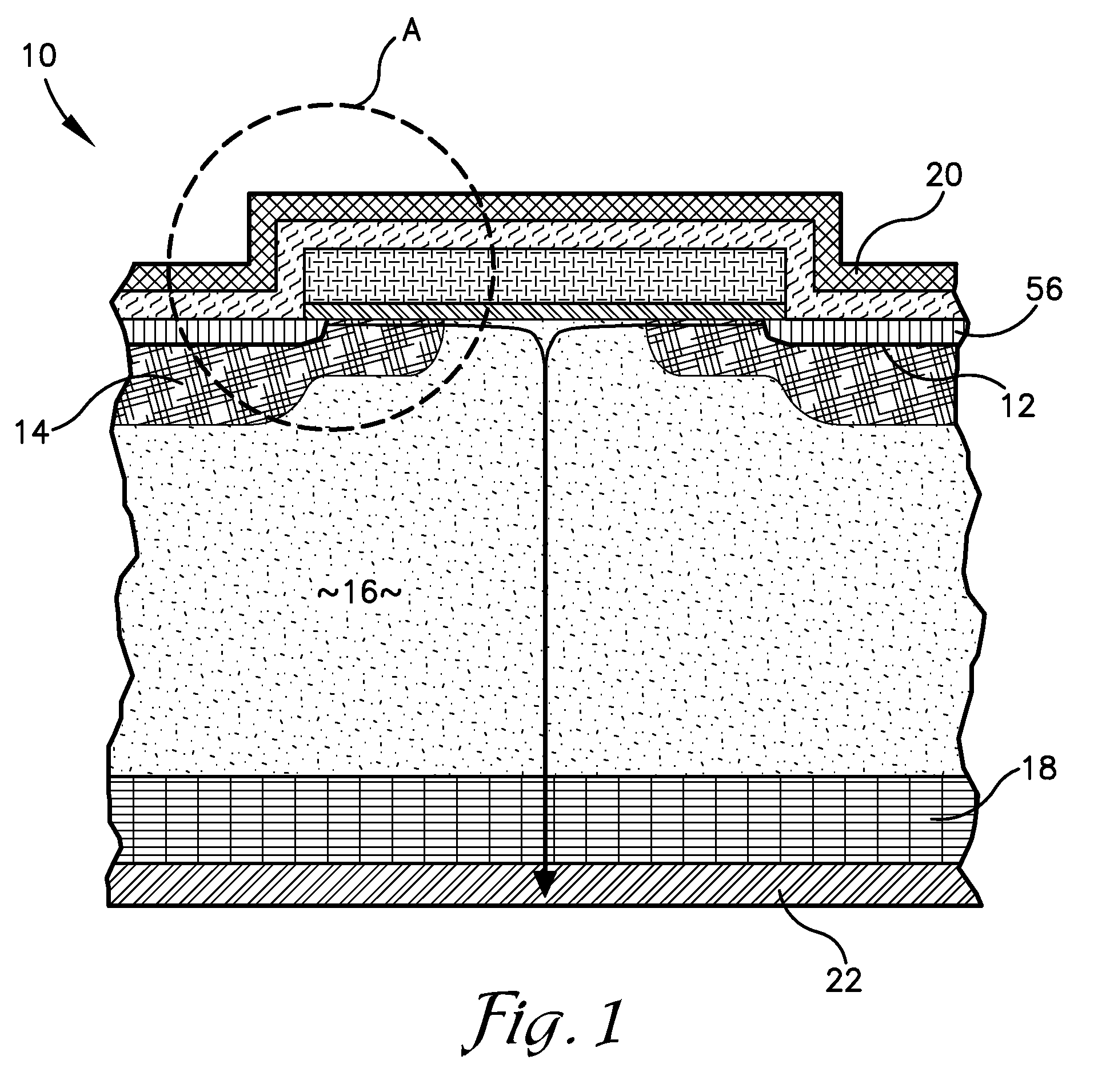
[0013]FIG. 1 is a fragmentary sectional elevation view of an embodiment of the device of the present invention;

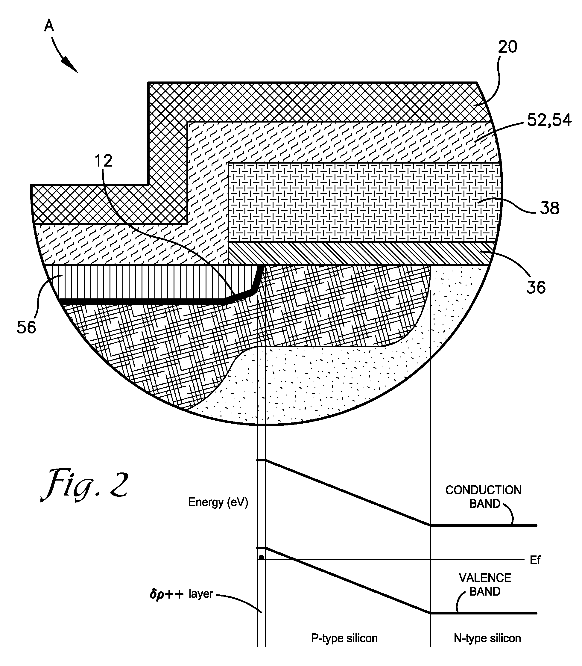
[0014]FIG. 2 is a fragmentary sectional elevation view of area A of the device of FIG. 1, wherein the device is in thermal equilibrium;

[0015]FIG. 3 is a fragmentary sectional elevation view of area A of the diode of FIG. 1, wherein the device is forward biased;

[0016]FIG. 4 is a fragmentary sectional elevation view of area A of the diode of FIG. 1, wherein the device is reverse biased;

[0017]FIG. 5 is a fragmentary sectional elevation view of the device following a first step in an embodiment of a method of fabricating the device.

[0018]FIG. 6 is a fragmentary sectional elevation view of the device following a second step;

[0019]FIG. 7 is a fragmentary sectional elevation view of...


PUM


Abstract

A high-efficiency power semiconductor rectifier device (10) comprising a δP++ layer (12), a P-body (14), an N-drift region (16), an N+ substrate (18), an anode (20), and a cathode (22). The method of fabricating the device (10) comprises the steps of depositing the N-drift region (16) on the N+ substrate (18), implanting boron into the N-drift region (16) to create a P-body region (14), forming a layer of titanium silicide (56) on the P-body region (14), and concentrating a portion of the implanted boron at the interface region between the layer of titanium silicide (56) and the P-body region (14) to create the δP++ layer (12) of supersaturated P-doped silicon.

Description

FIELD OF THE INVENTION[0001]The present invention relates to semiconductor devices and methods of making same. More specifically, the present invention relates to a power semiconductor rectifier device and a method of making same.BACKGROUND OF THE INVENTION[0002]Modern power circuits require power rectifiers with improved power switching performance. For high voltage applications, P+ / N rectifiers with high switching speeds are often used when high breakdown voltages and high operating temperatures are desired. For low voltage applications, Schottky barrier rectifiers are often used when high switching speeds and very low forward voltage drops are desired. The Schottky barrier rectifier is a majority carrier device which allows little reverse current flow during recovery. Unfortunately, Schottky barrier rectifiers suffer from undesirably high reverse leakage current when operating at elevated temperatures.[0003]Several modifications have been introduced to improve the blocking capabi...

Claims


Application Information

Patent Timeline
Patent Type & Authority Applications(United States)
IPC IPC(8): H01L31/00H01L21/425
CPCH01L29/0619H01L29/365H01L29/66136H01L29/66151H01L29/88H01L29/7391H01L29/861H01L29/8618H01L29/868H01L29/66356
Inventor HAMERSKI, ROMAN J.CHEN, ZERUIHONG, JAMES MAN-FAICHIEM, JOHNNY DUC VANHRUSKA, CHRISTOPHER D.EASTMAN, TIMOTHY
Owner DIODES INC
Why Eureka
Try Eureka