Method of Treating Non-Refrigerated, Spectrally-Selective Lead Selenide Infrared Detectors

a lead selenide, non-refrigerated technology, applied in the direction of optical radiation measurement, instruments, material analysis, etc., can solve the problems of low detachment efficiency, and high cost of both detectors to be cooled, so as to achieve low thermal expansion coefficient mismatch, good adhesion properties, and high detachment efficiency

Inactive Publication Date: 2008-09-18
MINIO DE DEFENSA
View PDF1 Cites 9 Cited by
  • Summary
  • Abstract
  • Description
  • Claims
  • Application Information

AI Technical Summary

Benefits of technology

[0004]Polycrystalline lead selenide is one of the oldest infrared detectors. It is a photonic detector, photoconductor type, sensitive to electromagnetic radiation of wavelengths up to 6 μm. Their most remarkable characteristics are: 1) it presents high detectivities at room temperature, 2) it is a fast detector (hundreds of kHz) 3) it is sensitive in the medium wave IR range (MWIR) and 4) it is cheap. The standard processing of polycrystalline lead selenide detectors is based on a chemical deposition process. During a long period of time this method has been considered as the most reliable method for processing polycrystalline lead selenide detectors, even though it presents important limitations: 1) it is compatible with a very limited number of substrates; 2) deposition of large polycrystalline clusters, makes necessary to use textured coatings which should have good adhesion properties with the substrate used, low thermal expansion coefficient mismatch...

Problems solved by technology

However, nowadays and due to fundamental and/or technological limitations the most of multicolour sensors are based in the technique of locating the IR detector on the focal plane of a wavelengths selector device (monochromator, interferometer, filters w...

Method used


Image

  • Method of Treating Non-Refrigerated, Spectrally-Selective Lead Selenide Infrared Detectors
  • Method of Treating Non-Refrigerated, Spectrally-Selective Lead Selenide Infrared Detectors
  • Method of Treating Non-Refrigerated, Spectrally-Selective Lead Selenide Infrared Detectors

Examples


Embodiment Construction

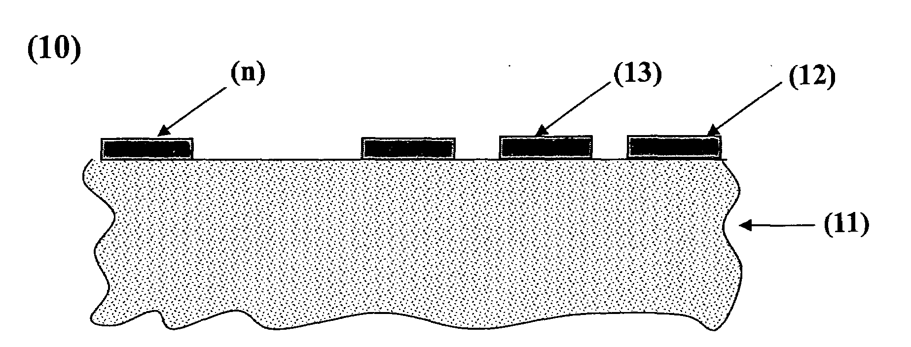
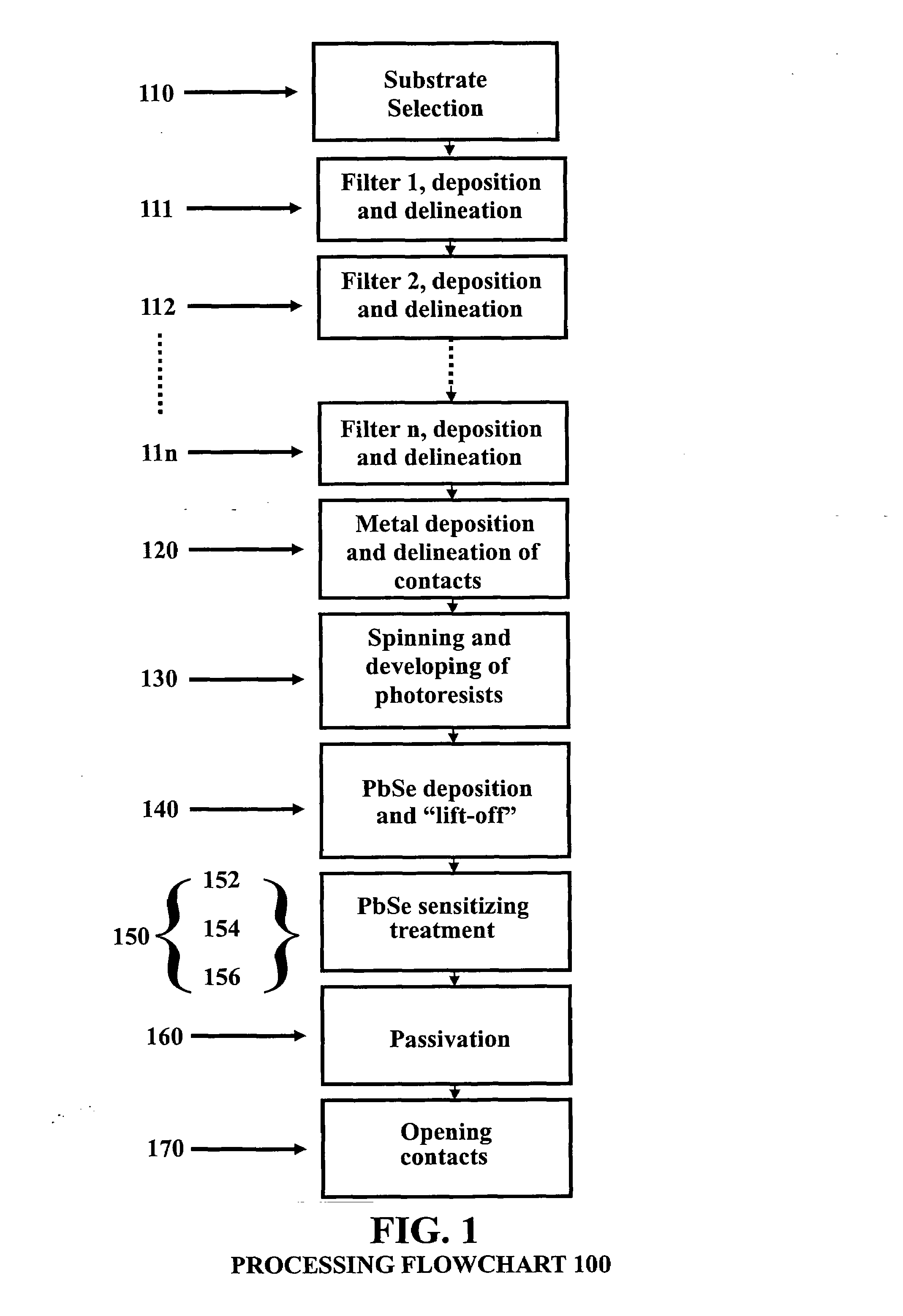
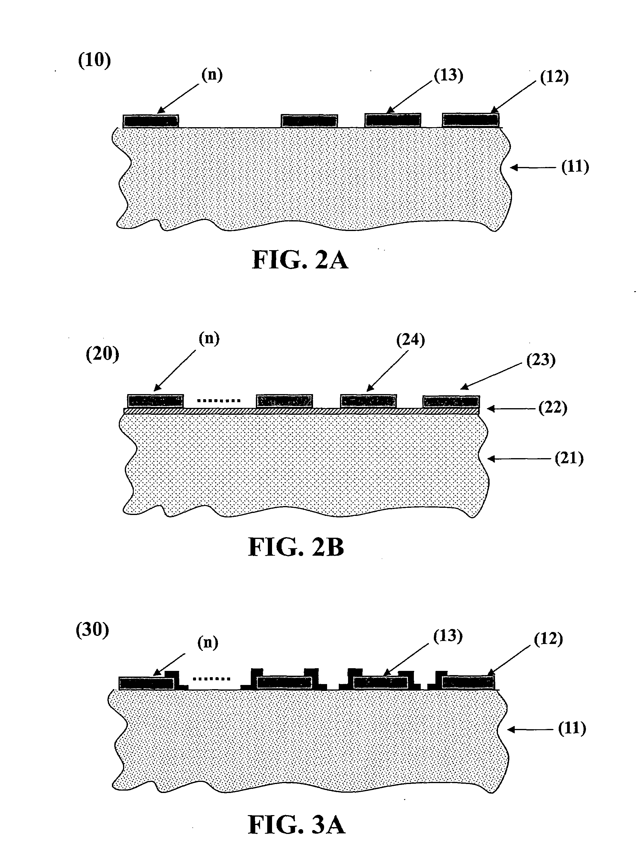
[0024]FIG. 1 shows a flowchart 100 illustrating one embodiment of the method to process multicolor polycrystalline lead selenide detectors. The method begins at step 110 by providing a suitable substrate; depending of the type of device to be processed the substrate material can be a dielectric material transparent to the medium wave infrared radiation (sapphire, . . . ) or a semiconductor material also transparent to the medium wave infrared radiation (silicon, germanium etc.). In this case it is necessary to diffuse or deposit a thin dielectric layer on their surface in order to avoid current leaks between sensors. The method continues at step 111 delineating and depositing layers corresponding to the first interference filter (color 1). Its delineation can be accomplished using mechanical masks or photolithography methods. Step 112 corresponds to delineation and deposition of second interference filter layers (color 2). Analogue to color 1 its delineation can be accomplished usin...


PUM


Abstract

The invention relates to a method of processing non-refrigerated lead selenide infrared detectors, consisting in: 1) selecting the substrate and preparing same; 2) delineating and depositing multilayer interference filters; and 3) treating polycrystalline lead selenide infrared detectors on the interference filters, comprising the following steps, namely 3a) metal deposition, 3b) delineation of the metal deposit, 3c) delineation of the sensor, 3d) PbSe deposition by means of thermal evaporation, 3f) processing of sensor, 3g) thermal treatment in order to sensitise the active material, and 3h) deposition of a passivator layer on the active material. The inventive method is unique in that it can be used to treat differently-shaped non-refrigerated infrared detectors on the same substrate, including discrete elements, multielements, linear matrices, two-dimensional matrices, etc., with the responses of each being modified by design by the corresponding interference filter. The invention is suitable for low-cost infrared detectors that are used for process control, gas analyses, temperature measurements, military applications, etc.

Description

OBJECT OF THE INVENTION[0001]It is a primary object of the present invention to provide a method to process multicolor polycrystalline lead selenide detectors based on substrate preparation, interference filters deposition and delineation followed of PbSe detectors processing on the interference filters. The method described is unique and clearly superior to others for processing uncooled multicolor IR infrared detectors. It is another object of this invention to provide a method to process improved single element polycrystalline lead selenide infrared detectors with the spectral selectivity feature monolithically integrated. It is yet another object of this invention to provide a method to process improved multielement polycrystalline lead selenide sensors with the spectral response of each detector modified as designed (multicolor sensor) and the spectral selectivity feature monolithically integrated. It is still another object of this invention to provide a method to process impr...

Claims


Application Information

Patent Timeline
IPC IPC(8): H01L31/0203H01L31/18
CPCH01L31/1032H01L31/02162H01L31/1037
Inventor OGANDO, GERMAN VERGARACARNEROS, ROSA ALMAZANZAZO, LUIS JORGE GOMEZHERCE, MARINA VERDUFERNANDEZ, PURIFICACION RODRIGUEZSUPERVIELLE, MARIA TERESA MONTOJO
Owner MINIO DE DEFENSA
Why Eureka
Try Eureka