Electronic device, display device, and semiconductor device and method for driving the same

a technology of display device and semiconductor device, which is applied in the direction of static indicating device, electroluminescent light source, instruments, etc., can solve the problems of high power consumption, high voltage applied to the light-emitting element, and high power consumption, so as to achieve a high ratio of light-emitting period and few variations of luminance

Active Publication Date: 2008-09-18
SEMICON ENERGY LAB CO LTD
View PDF98 Cites 141 Cited by
  • Summary
  • Abstract
  • Description
  • Claims
  • Application Information

AI Technical Summary

Benefits of technology

[0057]By using the present invention, variations of the current value caused by variations in the threshold voltage of a transistor can be suppressed. Therefore, desired current can be supplied to a load such as a lig...

Problems solved by technology

When the duty ratio is low, the amount of current supplied to a light-emitting element and a driving transistor is needed to be increased, so that voltage applied to the light-emitting element becomes higher and power consumption also becomes higher.
In addition, since the light-em...

Method used


Image

  • Electronic device, display device, and semiconductor device and method for driving the same
  • Electronic device, display device, and semiconductor device and method for driving the same
  • Electronic device, display device, and semiconductor device and method for driving the same

Examples


embodiment mode 1

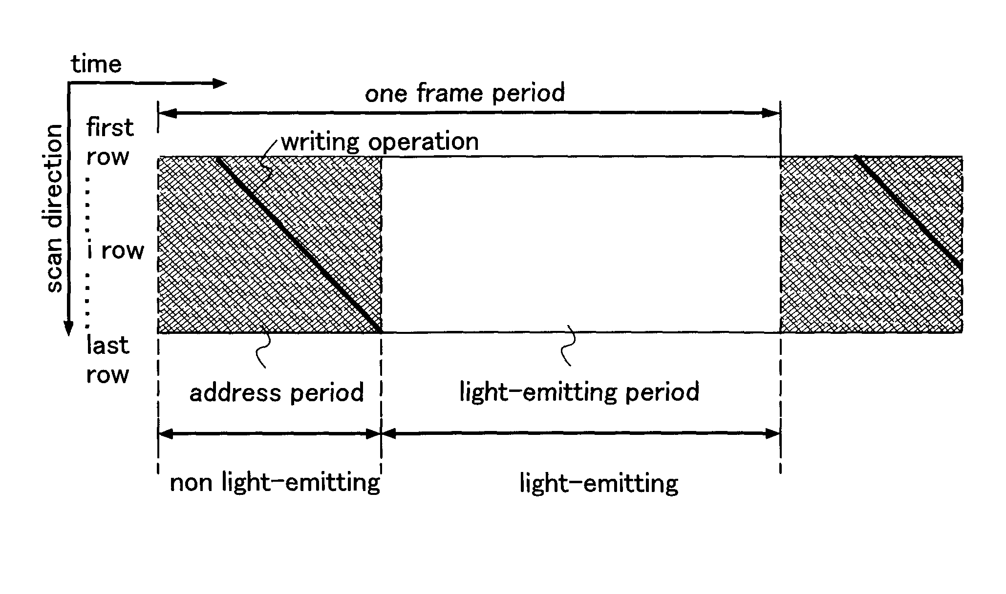
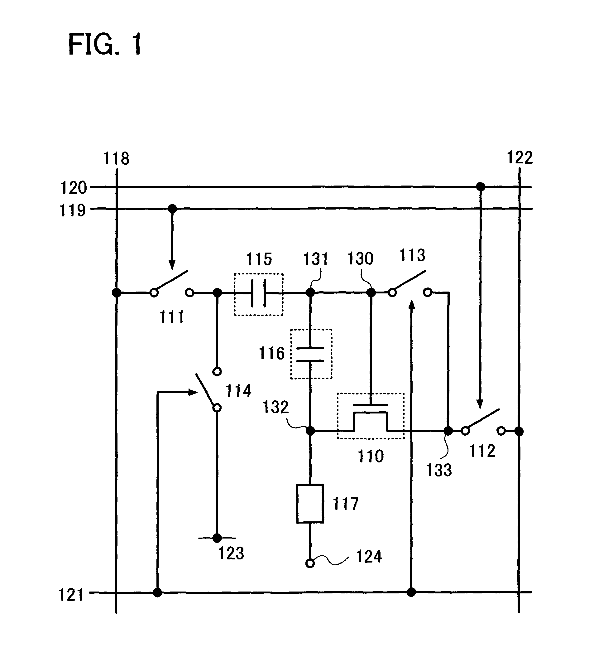
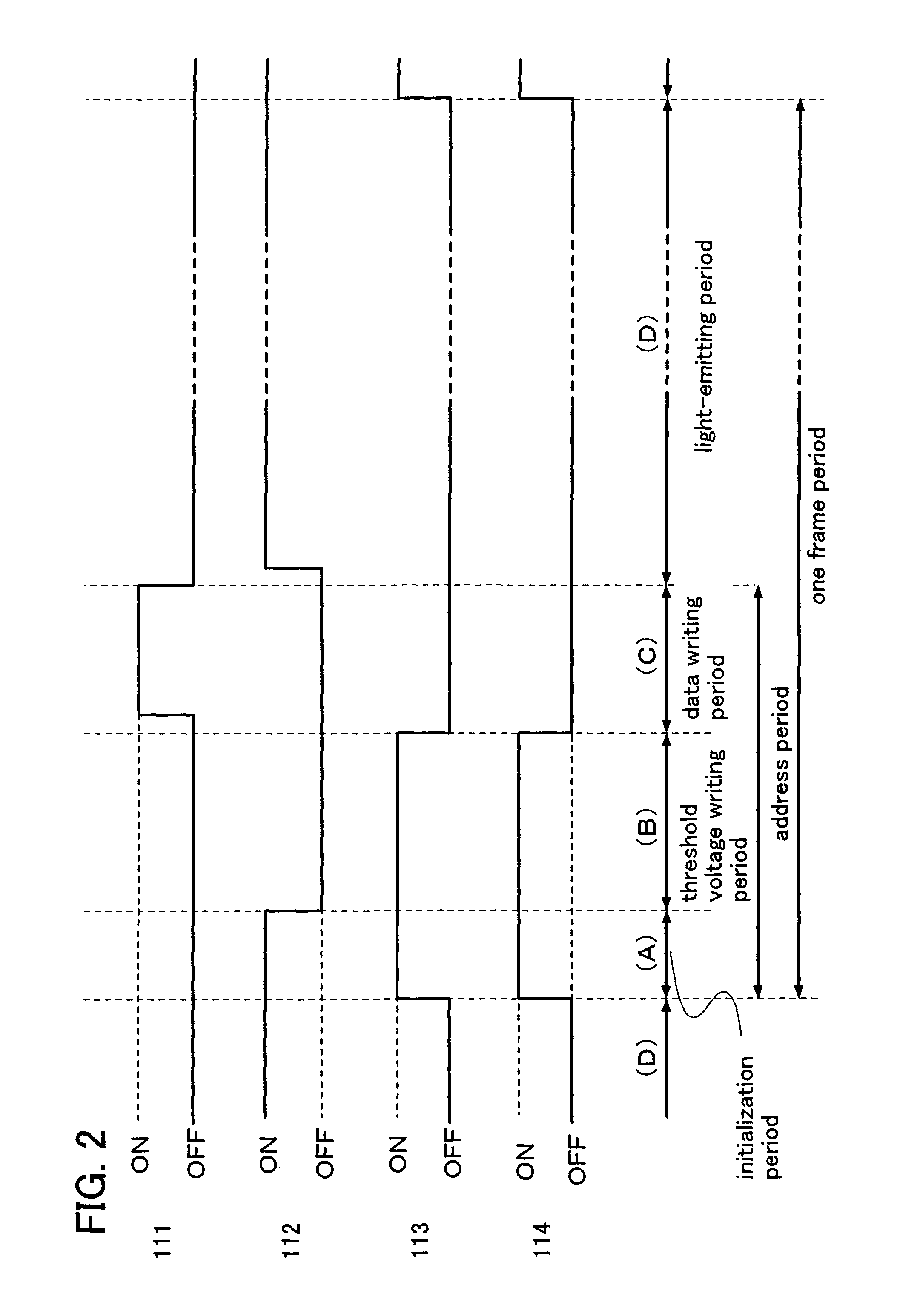
[0125]A basic structure of a pixel of the present invention is described with reference to FIG. 1. The pixel shown in FIG. 1 includes a transistor 110, a first switch 111, a second switch 112, a third switch 113, a fourth switch 114, a first capacitor 115, a second capacitor 116, and a light-emitting element 117. Note that the pixel is connected to a signal line 118, a first scan line 119, a second scan line 120, a third scan line 121, a power supply line 122, and a potential supply line 123. In this embodiment mode, the transistor 110 is an N-channel transistor, and is turned on when gate-source voltage (Vgs) thereof exceeds the threshold voltage (Vth). In addition, a pixel electrode of the light-emitting element 117 functions as an anode and an opposite electrode 124 thereof functions as a cathode. Note that gate-source voltage of the transistor is described as Vgs; drain-source voltage of the transistor is described as Vds; the threshold voltage of the transistor is described as ...

embodiment mode 2

[0184]In this embodiment mode, FIG. 9A shows a pixel having a structure which is different from that of Embodiment Mode 1. Note that portions which are similar to Embodiment Mode 1 are denoted by common reference numerals and detailed description of the same portions or portions having similar functions is omitted.

[0185]The pixel shown in FIG. 9A includes the transistor 110, the first switch 111, the second switch 112, the third switch 113, a rectifier 914, the first capacitor 115, the second capacitor 116, and the light-emitting element 117. Note that the pixel is connected to the signal line 118, the first scan line 119, the second scan line 120, a third scan line 921, a fourth scan line 922, and the power supply line 122. The pixel shown in FIG. 9A has a structure in which the rectifier 914 is used as the fourth switch 114 in FIG. 1, and the first electrode of the first capacitor 115 is connected to the fourth scan line 922 through the rectifier 914. That is, the rectifier 914 is...

embodiment mode 3

[0191]In this embodiment mode, FIGS. 10A and 10B, and FIG. 11 each show a pixel having a structure which is different from those of Embodiment Modes 1 and 2. Specifically, a pixel having a structure in which another wiring is substituted for the potential supply line 123 shown in FIG. 1 is described. Note that such a structure can be used because it is only necessary to supply a given potential to the first electrode of the first capacitor 115. Note that portions which are similar to Embodiment Mode 1 are denoted by common reference numerals and detailed description of the same portions or portions having similar functions is omitted.

[0192]The pixel shown in FIG. 10A includes the transistor 110, the first switch 111, the second switch 112, the third switch 113, the fourth switch 114, the first capacitor 115, the second capacitor 116, and the light-emitting element 117. Note that the pixel is connected to the signal line 118, the first scan line 119, the second scan line 120, the thi...


PUM


Abstract

A pixel having a transistor which controls a current value supplied to a load, a first storage capacitor, a second storage capacitor, and first to fourth switches is included. After the threshold voltage of the transistor is held in the second storage capacitor, a potential in accordance with a video signal is input to the pixel. Voltage obtained by adding a potential in which the potential in accordance with the video signal and the first storage capacitor are capacitively divided to the threshold voltage is held in the second storage capacitor in this manner, so that variation of a current value caused by variations in the threshold voltage of the transistor is suppressed. Thus, desired current can be supplied to the load such as a light-emitting element. In addition, a display device with little deviation from luminance specified by the video signal can be provided.

Description

BACKGROUND OF THE INVENTION[0001]1. Field of the Invention[0002]The present invention relates to a semiconductor device having a function for controlling current supplied to a load with a transistor, and relates to a display device including a pixel which is formed of a display element, luminance of which is changed in accordance with a signal, and a signal line driver circuit or scan line driver circuit which drives the pixel. In addition, the present invention relates to a driving method of such a semiconductor device and a display device. Further, the present invention relates to an electronic device having the display device in a display portion.[0003]2. Description of the Related Art[0004]In recent years, a self-luminous display device having a pixel formed by using a light-emitting element such as an electroluminescence (EL) element, i.e., a so-called to as light-emitting device has attracted attention. As a light-emitting element which is used for such a self-luminous display...

Claims


Application Information

Patent Timeline
IPC IPC(8): G06F3/038
CPCG09G3/2022H01L27/1255G09G2300/0426G09G2300/0439G09G2300/0465G09G2300/0819G09G2300/0852G09G2300/0861G09G2310/0251G09G2310/0262G09G2320/043G09G2320/045G09G2330/021H01L27/3244H01L27/1225G09G3/3233H05B33/10G09G2320/0233H10K59/12
Inventor KIMURA, HAJIMEYAMADA, TOMOKO
Owner SEMICON ENERGY LAB CO LTD
Why Eureka
Try Eureka