Mold, Method of Forming the Same, and Method of Producing Polycrystalline Silicon Substrate Using the Mold

Inactive Publication Date: 2008-09-25
KYOCERA CORP
View PDF52 Cites 11 Cited by
  • Summary
  • Abstract
  • Description
  • Claims
  • Application Information

AI Technical Summary

Benefits of technology

[0035]It is preferable that the pressing jig has a relief groove provided in an area corresponding to the outer corner of the mold such that the outer corner is not directly abutted thereagainst. The area corresponding to the outer corner is provided with the relief groove, so that the outer corner of the mold is prevented from being brought into contact with the pressing jig in attaching and detaching the pressing jig to and from the frame-shaped member. Even if attachment and detachment work is repeatedly performed, therefore, the outer corner can be prevented from being deformed and damaged, leading to reduction in the cost of the mold.
[0036]The frame-shaped member may have a projection abutted against the opposed lateral surface member for constraining displacement therebetween provided in its inner periphery. When the lateral surface member in the mold attempts to be deflected outward due to expansion caused by cooling and setting of the silicon melt, the displacement can be restrained by the projection.
[0037]It is preferable that when the engaging structure comprises engaging surfaces each comprising the projection of the one lateral surface member and the recess of the other lateral surface member engaged with and abutted against each other and being substantially level with the bottom surface of the bottom surface member, the frame-shaped members are respectively arranged at positions of the engaging surfaces. This can prevent the lateral surface member from being deflected even if stress is greatly applied to the lateral surface member as the frame-shaped member is fixed.
[0038]If the mold further comprises a mold release material applied to a mold inner surface comprising the bottom surface member and the lateral surface members, and four corners and eight ridges respectively serving as locking sections between the bottom surface member and the lateral surface members and locking sections between the lateral surface members, an inner

Problems solved by technology

The monocrystalline silicon solar cells have advantages that the conversion efficiencies thereof are easily improved because the qualities of substrates are good, while having disadvantages that the production costs of the substrates are high.
However, demands therefor have been increasing in recent years, so that high conversion efficiencies have been required at lower costs.
Such a integral-type mold 121 cannot be reused because the mold must be destroyed so as to take out a silicon ingot, so that the production cost of the silicon ingot is significantly high.
Therefore, a high-cost silicon raw material must be removed extra, so that the production cost of the silicon ingot is increased.
However, particularly a mold composed of molten silica is difficult to reuse because it is cracked due to differences in a temperature gradient and a sintered state within the mold in the process of cooling a block from a high-temperature state.
Further, a mold made of quartz is very difficult to reuse because it wears by its inner surface layer coated with a mold release material being changed into cristoblite and

Method used


Image

  • Mold, Method of Forming the Same, and Method of Producing Polycrystalline Silicon Substrate Using the Mold
  • Mold, Method of Forming the Same, and Method of Producing Polycrystalline Silicon Substrate Using the Mold
  • Mold, Method of Forming the Same, and Method of Producing Polycrystalline Silicon Substrate Using the Mold

Examples


example 1

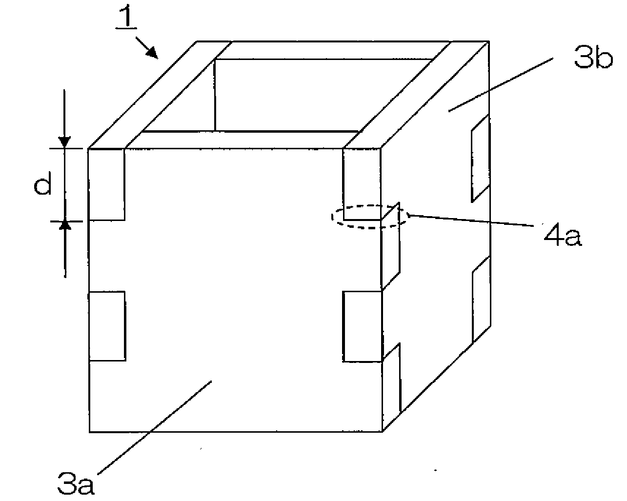
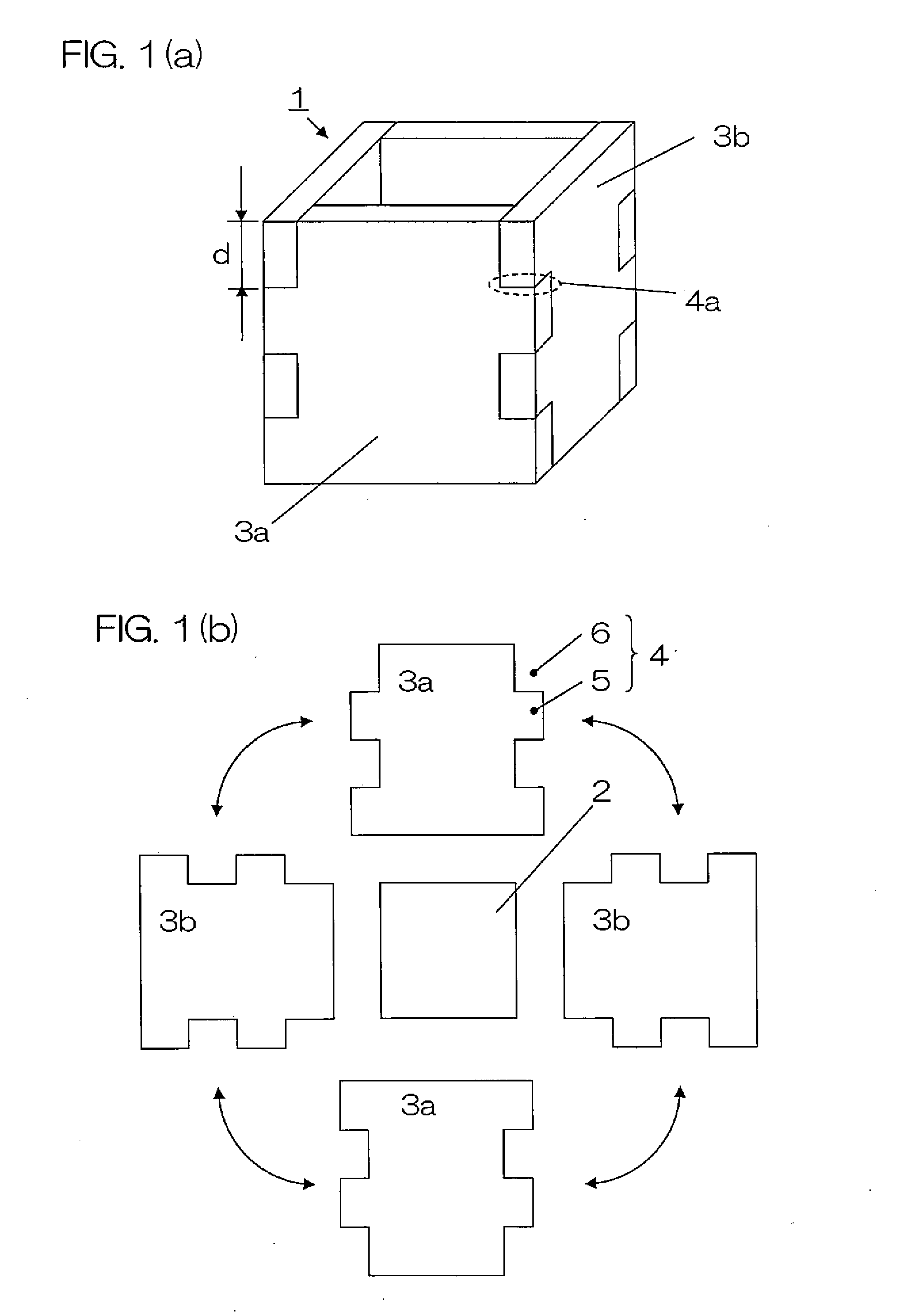
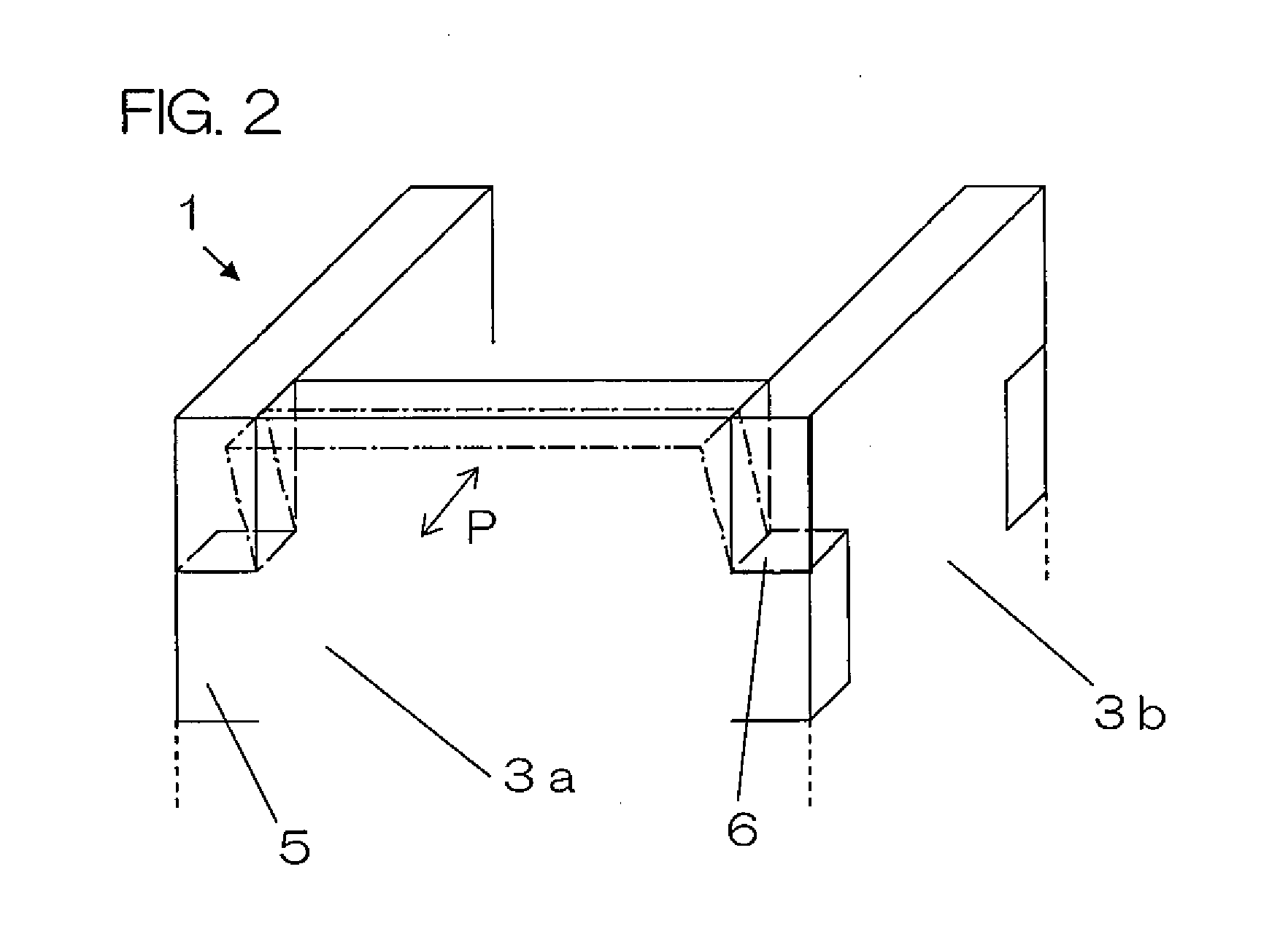
[0171]The mold in the conventional example shown in FIG. 17 and the mold having the configuration according to the present invention shown in FIG. 7 were compared with each other.

[0172]In the conventional example, one bottom surface member (20 mm in thickness) composed of graphite having a mold release material composed of silicon nitride applied thereto of 2 mm in thickness and four lateral surface members (20 mm in thickness) were assembled in a box shape, and were fixed using 32 assembling screws (φ5 mm by 40 mm in length), to obtain a mold (220 mm by 220 mm in inside dimensions by 250 mm in height).

[0173]Twenty-two kg of a silicon melt was poured into the obtained mold, the top of the mold was heated to 1460° C. in an argon (Ar) atmosphere whose pressure was reduced to 100 Torr, the temperature of the mold was gradually lowered from the bottom of the mold to solidify the silicon melt in one direction, to obtain a silicon ingot having a height of approximately 200 mm.

[0174]In the...

example 2

[0179]The mold in the conventional example shown in FIG. 17 and the mold having the configuration according to the present invention shown in FIG. 13 were compared with each other.

[0180]In the conventional example, one bottom surface member (20 mm in thickness) composed of graphite having a mold release material composed of silicon nitride applied thereto of 2 mm in thickness and four lateral surface members (20 mm in thickness) were assembled in a box shape, and were fixed using 40 assembling screws (φ5 mm by 40 mm in length), to obtain a mold (350 mm by 350 mm in inside dimensions by 350 mm in height).

[0181]Eighty-five kg of a silicon melt was poured into the obtained mold, the top of the mold was heated to 1460° C. in an argon (Ar) atmosphere, whose pressure was reduced to 100 Torr, the temperature of the mold was gradually lowered from the bottom of the mold to solidify the silicon melt in one direction, to obtain a silicon ingot having a height of approximately 300 mm.

[0182]In ...


PUM

PropertyMeasurementUnit
Distanceaaaaaaaaaa
Distanceaaaaaaaaaa
Lengthaaaaaaaaaa

Abstract

Disclosed is a mold wherein one bottom surface member (2) and four lateral surface members (3) are assembled. The sides of each lateral surface member (3) are respectively provided with a projection (5) and a recess (6) for combining the lateral surface members together, and the projection (5) of one lateral surface member (3) is engaged with the recess (6) of the adjacent lateral surface member (3). By using the one bottom surface member (2) and four lateral surface members (3), a mold can be assembled or disassembled without using screw or bolts. Consequently, the assembly or disassembly work of the mold is dramatically simplified, thereby improving work efficiency significantly.

Description

FIELD OF THE INVENTION[0001]The present invention relates to a mold suited to cast a polycrystalline silicon ingot used for a silicon substrate for a solar cell, for example, and more particularly to a mold, which can be assembled and dissembled, comprising one bottom plate and four side plates and a method of forming the same, and a method of producing a polycrystalline silicon substrate using the mold.DESCRIPTION OF RELATED ART [0002]Practical application of solar cells is expected in a wide field from small-scale domestic purposes to large-scale power generating systems as clean sources of alternative energy to oil. The solar cells are classified into system, such as crystalline, amorphous, and compound depending on the type of raw material to be used. Among them, many of the solar cells currently in the marketplace are crystalline silicon solar cells. The crystalline silicon solar cells are further classified into monocrystalline types and polycrystalline types. The monocrystall...

Claims


Application Information

Patent Timeline
IPC IPC(8): B22C9/00C01B33/02
CPCB22C9/00C01B33/02Y10T117/1092Y10T117/106Y10T117/1052Y02E10/50C01B33/00C30B15/34H01L31/04
Inventor SAKAI, YOUHEIAMANO, YOSHIYUKI
Owner KYOCERA CORP
Why Eureka
Try Eureka