Bolometer-type thz-wave detector

a detector and thz wave technology, applied in the field of detectors, can solve the problems of lowering yield, difficult to set the gap within the range of 0.1 to 1 m, and difficult to set the gap within the range of 0.2 to 1 m, so as to achieve high yield, improve absorption of thz wave, and achieve high yield.

Active Publication Date: 2008-10-02
NEC CORP +2
View PDF4 Cites 39 Cited by
  • Summary
  • Abstract
  • Description
  • Claims
  • Application Information

AI Technical Summary

Benefits of technology

[0018]As mentioned above, in the present invention, the gap between the reflective film and the temperature detecting portion is set on the basis of the wavelength of infrared, and the sheet resistance of the temperature detecting portion is set on the basis of the THz wave. Thus, the absorptance of the THz wave can be remarkably improved using the structure and manufacturing method of an infrared detector, by which a high-performance THz-wave detector can be manufactured with a high yield.
[0019]According to the present invention, a high-performance bolometer-type THz-wave detector can be manufactured with a high yield.

Problems solved by technology

However, if the detecting element 27 is to be floated from the glass layer 21 by the leg 28 using the MEMS (Micro-Electro-Mechanical Systems) technology, it is difficult to set the gap within the range of 0.1 to 1 μm, and there is a problem that yield is lowered.
However, if the heater film 23 is to be floated from the glass layer 21 using the MEMS technology, it is difficult to set the gap within the range of 0.2 to 1 μm, and there is a problem that yield is lowered.
It is extremely difficult to incorporate the detecting element 27 in such a small region of several μm, and there is a problem that the yield is further deteriorated.

Method used


Image

  • Bolometer-type thz-wave detector
  • Bolometer-type thz-wave detector
  • Bolometer-type thz-wave detector

Examples


example 1

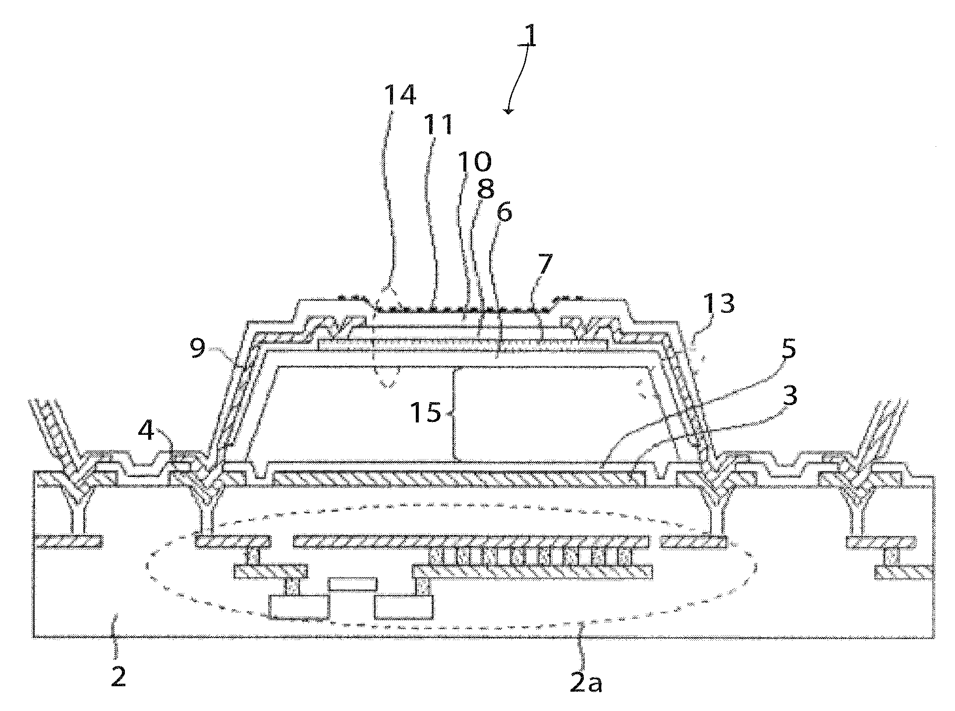
[0050]In order to describe the above embodiment in more detail, a bolometer-type THz-wave detector according to the first embodiment of the present invention will be described referring to FIGS. 1 to 7B.

[0051]As shown in FIG. 1, a bolometer-type THz-wave detector 1 of this embodiment has, on a circuit substrate 2 having a read-out integrated circuit 2a and the like, a reflective film 3 reflecting an incident THz wave and a contact 4 connected to the read-out integrated circuit 2a are formed, and on top of that, a first protective film 5 is formed. On the contact 4, a supporting portion 13 comprising a second protective film 6, a third protective film 8, an electrode wiring 9, and a fourth protective film 10 is formed. The electrode wiring 9 is connected to the read-out integrated circuit 2a through the contact 4. By the supporting portion 13, a temperature detecting portion 14 (diaphragm) comprising the second protective film 6, a bolometer thin film 7, the third protective film 8, ...

example 2

[0071]Next, the bolometer-type THz-wave detector according to a second embodiment of the present invention will be described referring to FIGS. 8 to 10.

[0072]As shown in FIG. 8, the bolometer-type THz-wave detector 1 of this embodiment has, on the circuit substrate 2 having the read-out integrated circuit 2a and the like, the reflective film 3 reflecting the incident THz wave and the contact 4 connected to the read-out integrated circuit 2a formed, and the first protective film 5 is formed on top of it. On the contact 4, the supporting portion 13 comprising the second protective film 6, the third protective film 8, the electrode wiring 9, and the fourth protective film 10 is formed. The electrode wiring 9 is connected to the read-out integrated circuit 2a through the contact 4. By the supporting portion 13, the temperature detecting portion 14 (diaphragm) comprising the second protective film 6, the bolometer thin film 7, the third protective film 8, the fourth protective film 10, a...

example 3

[0083]Next, the bolometer-type THz-wave detector according to a third embodiment of the present invention will be described referring to FIGS. 11 to 15B.

[0084]In the bolometer-type THz-wave detector of the present invention, in order to form the optical resonance structure suitable for the THz wave, the gap between the reflective film 3 and the temperature detecting portion 14 is preferably wider. On the other hand, if the gap between the reflective film 3 and the temperature detecting portion 14 is made wider, the formation or removal of the sacrifice layer 17 becomes difficult. Then, in this embodiment, by interposing a member with a predetermined refractive index (referred to as an optical film 16) between the reflective film 3 and the temperature detecting portion 14, the optical path length with the refractive index considered is changed.

[0085]It is only necessary that the optical film 16 is a member with a large refractive index, a small absorption of the THz wave and favorabl...


PUM

PropertyMeasurementUnit
wavelengthaaaaaaaaaa
frequencyaaaaaaaaaa
sizeaaaaaaaaaa

Abstract

In a micro-bridge structure in which a temperature detecting portion (diaphragm) including a bolometer thin film is supported by a supporting portion in a state floated from a circuit substrate, a reflective film reflecting a THz wave is formed on the circuit substrate, an absorbing film absorbing the THz wave is formed on the temperature detecting portion, and an optical resonance structure is formed by the reflective film and temperature detecting portion. A gap between the reflective film and temperature detecting portion measures approximately ¼ infrared wavelength (e.g., 1.5 to 2.5 μm). Sheet resistance of the temperature detecting portion is set in a range in which an absorptance of the THz wave becomes a predetermined value or above on the basis of the THz wave (approximately 10-100 Ω/sq.). The absorptance of the THz wave is drastically improved while using the structure and manufacturing technique of a bolometer-type infrared detector.

Description

BACKGROUND OF THE INVENTION[0001]1. Field of the Invention[0002]The present invention relates to a detector for detecting an electromagnetic wave (THz-wave) in a THz-frequency band and more particularly to a bolometer-type THz-wave detector.[0003]2. Description of the Related Art[0004]Recently, an electromagnetic wave in a terahertz frequency band between light and an electromagnetic wave (that is, an electromagnetic wave with a frequency of 1012 Hz and a wavelength of approximately 30 μm to 1 mm, hereinafter referred to as THz-wave) has drawn attention as the electromagnetic wave directly reflecting information of a substance. A detector for detecting the THz wave (hereinafter referred to as a THz-wave detector) is generally in a structure comprising an antenna portion such as a dipole antenna or a Bow-tie antenna capturing the THz wave and an electric signal conversion portion for converting the THz wave captured by the antenna portion into an electric signal. As methods of conver...

Claims


Application Information

Patent Timeline
Patent Type & Authority Applications(United States)
IPC IPC(8): G01J5/00G01J1/02G01J5/20G01N21/35G01N21/3581
CPCG01J5/02G01J5/0215G01J5/0235G01J5/024G01J5/20G01J5/08G01J5/0809G01J5/0815G01J5/0837G01J5/046G01J5/0808
Inventor ODA, NAOKIKOMIYAMA, SUSUMUHOSAKO, IWAO
Owner NEC CORP
Why Eureka
Try Eureka