Semiconductor light emitting device and nitride semiconductor light emitting device

a light emitting device and semiconductor technology, applied in the field of nitride semiconductor light emitting devices, can solve the problems of difficult to convert the well layer into a p-type, large activation energy of a p-type impurity, etc., to achieve high light emission efficiency, suppress the deterioration of the crystallinity of the active layer, and high current density

Inactive Publication Date: 2008-10-02
SHARP KK
View PDF4 Cites 4 Cited by
  • Summary
  • Abstract
  • Description
  • Claims
  • Application Information

AI Technical Summary

Benefits of technology

[0027]According to the present invention, a semiconductor light emitting device and a nitride semiconductor light emitting device can be provided which are capable of suppressing the deterioration of crystallinity of an active layer and have high light emitting efficiency and high current density.

Problems solved by technology

However, the activation energy of a p-type impurity is very large in a semiconductor.
Further, in the case of using an InGaN layer in a well layer of multiple quantum well structure of the nitride semiconductor active layer in the nitride semiconductor light emitting device described in Japanese Patent Laying-Open 2004-064080, since it is necessary to form the layer at a low temperature due to extremely high vapor pressure of In, it is difficult to activate the well layer into a p-type at such a low temperature.

Method used


Image

  • Semiconductor light emitting device and nitride semiconductor light emitting device
  • Semiconductor light emitting device and nitride semiconductor light emitting device
  • Semiconductor light emitting device and nitride semiconductor light emitting device

Examples


example 1

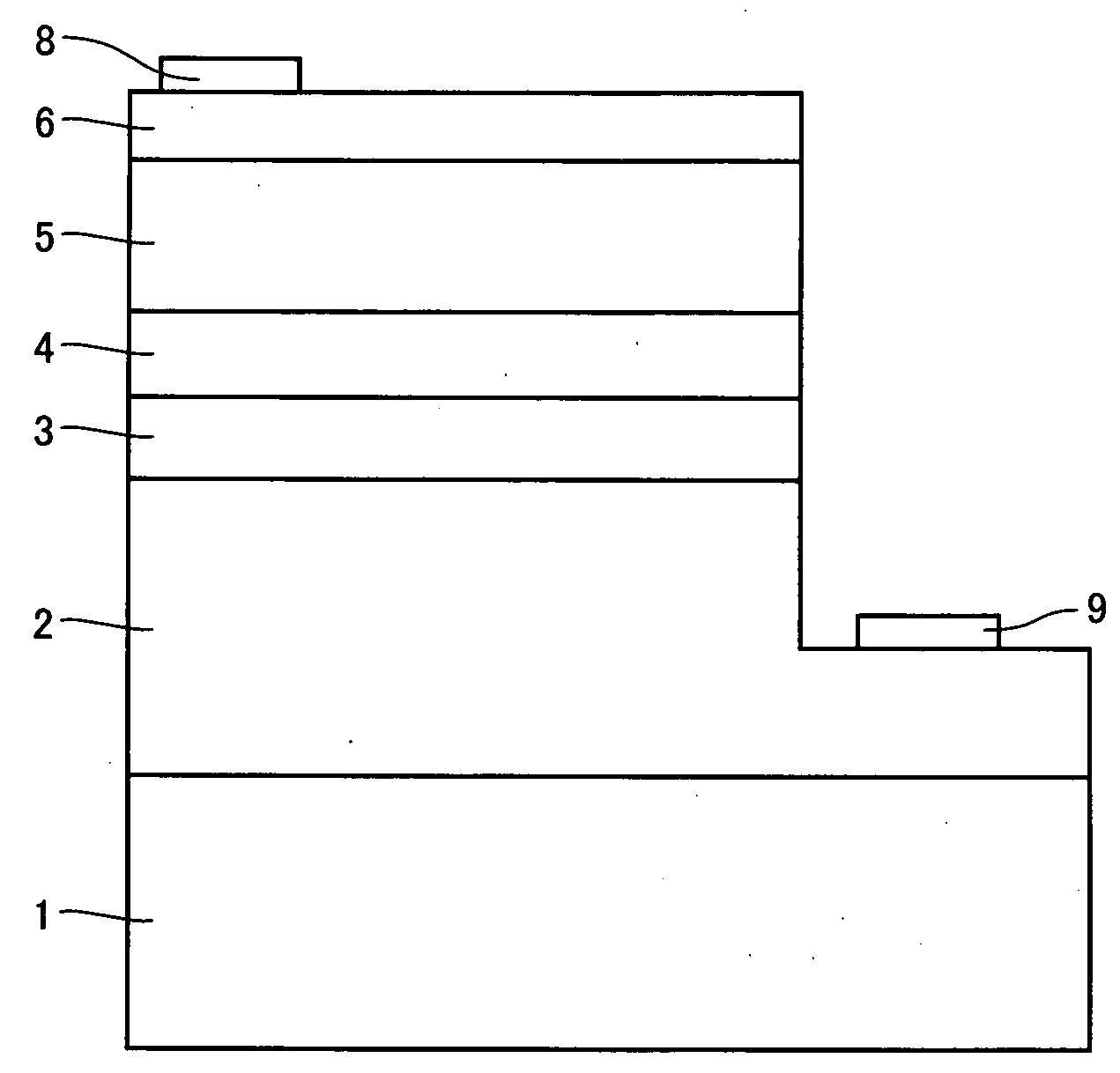
[0073]In Example 1, the nitride semiconductor light emitting diode having a configuration shown in the schematic cross-sectional view of FIG. 4 was manufactured.

[0074]First, a sapphire substrate 101 was set in a reaction furnace of a MOCVD machine. Then, the temperature of sapphire substrate 101 was raised to 1050° C. while hydrogen flowed in the reaction furnace, to perform cleaning of the surface (C face) of sapphire substrate 101.

[0075]Next, the temperature of sapphire substrate 101 was lowered to 510° C. and hydrogen as carrier gas and ammonia and TMG (trimethyl gallium) as raw material gas flowed in the reaction furnace, to grow a GaN buffer layer 102 on the surface of sapphire substrate 101 (C face) to a thickness of about 20 nm with a MOCVD method.

[0076]The temperature of sapphire substrate 101 was raised to 1050° C. and hydrogen as carrier gas, ammonia and TMG as raw material gas, and silane as impurity gas flowed in the reaction furnace, to grow an n-type GaN under-layer 10...

example 2

[0087]With the same conditions and the same method as in Example 1, n-type GaN contact layer 104 was grown.

[0088]Next, the temperature of sapphire substrate 101 was kept to 1050° C. and hydrogen as carrier gas, ammonia, TMG, and TMA (trimethyl aluminum) as raw material gas, and CP2Mg as impurity gas flowed in the reaction furnace, to grow an p-type Al0.25Ga0.75N layer doped with Mg at a concentration of 1×10¹⁹ / cm3 on n-type GaN contact layer 104 to a thickness of 20 nm with a MOCVD method.

[0089]Then, the temperature of sapphire substrate 101 was kept to 1050° C. and hydrogen as carrier gas, ammonia and TMG as raw material gas, and CP2Mg as impurity gas flowed in the reaction furnace, to grow a p-type GaN layer doped with Mg at a concentration of 1×10¹⁹ / cm3 on the p-type Al0.25Ga0.75N layer to a thickness of 10 nm with a MOCVD method.

[0090]After that, a nitride semiconductor light emitting diode device in Example 2 was manufactured by performing steps after the growth of active layer...

example 3

[0094]With the same conditions and the same method as in Example 1, n-type GaN contact layer 104 was grown.

[0095]Next, the temperature of sapphire substrate 101 was kept to 1050° C. and hydrogen as carrier gas, ammonia, TMG, and TMA as raw material gas, and CP2Mg as impurity gas flowed in the reaction furnace, to grow a p-type Al0.25Ga0.75N layer on n-type GaN contact layer 104 to a thickness of 20 nm with a MOCVD method.

[0096]Then, the temperature of sapphire substrate 101 was kept to 1050° C. and hydrogen as carrier gas, and ammonia and TMG as raw material gas flowed in the reaction furnace, to grow an undoped GaN layer on the p-type Al0.25Ga0.75N layer to a thickness of 20 nm with a MOCVD method.

[0097]After that, the nitride semiconductor light emitting diode device in Example 3 was manufactured by performing steps after the growth of active layer 106 with the same conditions and the same method as in Example 1.

[0098]In the relationship between the current density and the light e...


PUM


Abstract

The present invention is a semiconductor light emitting device including an n-type semiconductor layer, an active layer, a first p-type semiconductor layer between the n-type semiconductor layer and the active layer, and a second p-type semiconductor layer on the opposite side of the first p-type semiconductor layer from the active layer. Further, the present invention is a nitride semiconductor light emitting device including an n-type nitride semiconductor layer, a nitride semiconductor active layer, a first p-type nitride semiconductor layer between the n-type nitride semiconductor layer and the nitride semiconductor active layer, and a second p-type nitride semiconductor layer on the opposite side of the first p-type nitride semiconductor layer from the nitride semiconductor active layer.

Description

[0001]This nonprovisional application is based on Japanese Patent Application No. 2007-085146 filed with the Japan Patent Office on Mar. 28, 2007, the entire contents of which are hereby incorporated by reference.BACKGROUND OF THE INVENTION[0002]1. Field of the Invention[0003]The present invention relates to a semiconductor light emitting device and a nitride semiconductor light emitting device, and particularly relates to a semiconductor light emitting device and a nitride semiconductor light emitting device which are capable of suppressing the deterioration of crystallinity of an active layer and have high light emitting efficiency and high current density.[0004]2. Description of the Background Art[0005]The structure of a conventional nitride semiconductor light emitting device is generally a structure in which an n-type nitride semiconductor layer, an n-type or an undoped nitride semiconductor active layer, and a p-type nitride semiconductor layer are layered in this order on a s...

Claims


Application Information

Patent Timeline
Patent Type & Authority Applications(United States)
IPC IPC(8): H01L33/00H01L33/32H01L33/06
CPCH01L33/02H01L33/04H01L33/32
Inventor KOMADA, SATOSHI
Owner SHARP KK
Why Eureka
Try Eureka